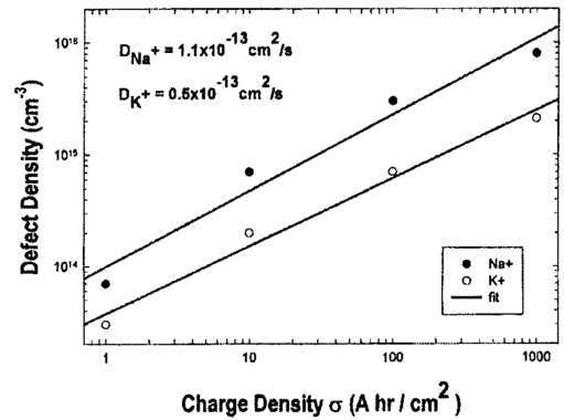
1.IntroductionNew optical techniques in biotechnology have arisen with the advent of new materials, laser sources, advances in surface chemistry and molecular biology. These developments have enabled the creation of microelectromechanical system (bioMEM) devices for inexpensive, small, fast, diagnostic tools for biomedical analysis.1 Among these new devices are microfluidic structures that allow rapid analyses of biomolecules, biological cells, and micro-organisms.2 3 It has recently been shown that compound semiconductors have ideal light-emitting characteristics for probing biological systems. Compounds such as GaAs, AlGaAs, and AlGaN have potential for new biomedical applications such as photodynamic therapy, optical tomography, cell micromanipulation, and in vivo laser cytometry. They are very attractive because of their capability to generate, transmit, modulate, and detect light over a wide range of wavelengths from the ultraviolet, visible, and near infrared. These semiconductors emit light at wavelengths where tissues and cells are highly transparent, in the so called “therapeutic window.” 4 Wider band gap materials can emit in the ultraviolet where nucleic acids and proteins absorb, or in the visible where aromatic compounds and molecular probes absorb. Newly developing photonic lattices and surface-emitting materials may be especially useful because of their porous structure and novel surface-emitting geometry that allows easy integration with molecular recognition chemistry and polymer overlayers for spectroscopy of biomolecules, cells, and micro-organisms. The fundamental issues here are the development of synthesis and lithography techniques for controlling the ultrasmall dimensions of the layers and lattice constant, and the functionalization of the semiconductor surfaces. Recently, our research on semiconductors has spawned an entirely new class of microcavity structures useful for biomedical and environmental sensing applications. The structures are microcavities formed by integrating a semiconductor Bragg heterostructure with a micropatterned dichroic glass flow chip.5 6 7 These structures are optically resonant cavities that can emit spontaneous or stimulated light. Solutions of the Helmholtz equation reveal intense optical fields generated in these microcavities that are sensitive to the optical properties of materials placed inside the cavity. The resonant light frequencies emitted from the cavity are sensitive to both the real and imaginary components of the complex dielectric constant. Biological fluids or cells that pass through the cavity can be identified by the spectral changes in the emitted light spectrum. Synthesis and Study of Biocompatible Materials InterfacesBefore such microfluidic structures can be used in a practice, a formidable scientific and technical barrier must be overcome. The barrier is the fact that many of the materials under consideration for biosensing and biomedical platforms are incompatible with the biochemistry of cells and molecular species contained in aqueous solution. There are several major hurdles that must be cleared before these materials that form the micro- and nanostructures can become useful in medical applications. For example, modified material surfaces must be developed for reliably transporting biofluids across materials surfaces at high speed while minimizing the effects of surface tension and nonspecific protein adhesion. These fluids include pH buffered saline solutions, cell growth media, antibodies, cytokines, enzymes, as well as the molecules, cells and extracellular matrix attending the cells. The fluids must not degrade the electronic, optical, or mechanical performance nor corrode material surfaces. Proteins and cells must traverse material surfaces without sticking to the surface and limiting the flow of the biofluid. The materials surfaces must be passivated with inert materials that will not alter the physiology of the cells yet be robust enough to withstand enzymes that may attack them. Further, methods for sealing the dissimilar materials to form micro- and nanocavities must be developed to isolate fluids and prevent cross contamination from adjacent flow channels. The integrity of these seals must be retained over the lifetime of the structure such that the physical dimensions of the micro- or nanocavity remain constant. Fundamental questions arise as to how to tailor the interface between the material and biosystem. Is it possible to use successive transitional layers between the material surface and a cell lipid membrane to gradually change the material characteristics from inorganic to organic? What materials should be chosen? What is the nature of the atomic level binding at the interface? How could the integrity of each material interface be preserved when exposed to various kinds of biofluids? Can the interface be functional as well as structural? What kind of transduction mechanisms can be produced in the substrate material, interfaces, or surface material to study the biosystem? Can the transduction mechanism be made specific and highly sensitive to a particular molecule or cell? If such interfaces can be developed, it would enable platforms that integrate a microfluidic-optical detection system on a chip, for example, for whole blood measurements that can probe the immune system response to pathogens. 2.Materials Biocompatiblity IssuesToday many different materials are used in the human body or in contact with cultured tissues or cells for a variety of purposes and requirements for biocompatibility. Most often, the interface requirements involve mechanical attachment of cells to a substrate, or hydrophilic/hydrophobic requirements for fluidics, or minimizing toxicity to the living structure. Recently, materials used in silicon-based MEMS devices have been analyzed for biocompatiblilty.8 Also, biocompatibility of implantable microelectronic silicon devices has recently been reported in the literature.9 In the present work we are concerned with a relatively new additional requirement: that the biofluid does not degrade the optoelectronic properties of a semiconductor material. We believe this study may be one of the first to address this issue. Optoelectronic properties are particularly sensitive to material quality through the incorporation of impurity atoms that can arise from contact with a biofluid. Thus, studies of optoelectronic degradation can provide insight into the fundamental mechanisms of degradation that any electronic material in contact with a biosystem must endure. There are a number of interactions between a biosystem and a material that merit consideration. Figure 1 is a schematic diagram of a hypothetical system comprising cells in a biofluid in contact with a material surface. In the fluid are various analytes including proteins, enzymes, ions, and water molecules. Each one of these species can interact with the surface. For example, cells and proteins can absorb onto the surface. Enzymes can catalyze dissolution of the surface material. Water molecules can be adsorbed on or migrate into the material. Further, ions in solution can be conducted by surface fields into the material. Each one of these interactions will have particular consequences on the overall lifetime, robustness, and functionality of the material. Figure 1Schematic of the types of interactions between a material surface and a biofluid. Different cellular, molecular, and ionic species are labeled.  On the other hand, the atomic or molecular species in the material can have significant interactions with the biosystem. For example, the lattice atoms of a semiconductor can be dissolved and incorporated into organelles of cells and inhibit metabolic pathways. Or, they can change the pH or ionic strength of the biofluid. The upper micrograph in Figure 2 shows the influence of a gallium arsenide surface on the cell structure of a rat lung epithelial cell that attempted to adhere and grow. The cell appeared to be unable to find a suitable area on which to attach, grow, and divide. Instead, it became very flat and splayed out across the surface before it underwent necrosis. In contrast, the same cell types were able to grow and proliferate on a similar wafer of GaAs that had been coated with a thin (∼100 nm) layer of SiO 2. Similar micrographs were recorded with several III–V compound semiconductor wafers, including ones of GaAs, GaP, GaSb, InAs, InP, InSb, Si, and Ge. The compounds comprising Ga atomic species were the most detrimental to cell growth. Presumably, the Ga incorporates into a critical molecule in the metabolic pathway and inhibits cell growth. Thus, it is important to find surface coatings and functional layers that minimize exposure to this heavy metal atom. Figure 2Optical micrographs of rat lung epithelial cells cultured on (upper photo) a bare GaAs wafer and (lower photo) GaAs coated with SiO 2.  The human body is composed by weight percentage of the following predominant atomic species: O 65, C 18.5, H 9.5, Ca 1.5, P 1.0, K 0.4, S 0.3, Na 0.2, Cl 0.2, and Mg 0.1. In the work described below, we consider the role of several of these species, oxygen, carbon, sodium, chlorine, and potassium, on biocompatibility with compound semiconductor optoelectronic materials. These species are derived from phosphate buffered salt (PBS) solutions which are frequently used as a flow medium for cells because of the pH stability and osmotic compatibility. The PBS solution, obtained from the Biofluids Division of Biosource International, was pH 7.2 and contained 2320 mg/L potassium phosphate (KH 2 PO 4), 90 000 mg/L sodium chloride (NaCl), and 7030 mg/L sodium phosphate (NaH 2 PO 4). The solute species are concentrated in full strength aqueous solution to near 1020 cm −3, about two orders of magnitude lower than the atomic concentration of the semiconductor crystal. The solution was diluted in de-ionized water to control the specie concentration. 3.Surface Functionalization of Semiconductors3.1.Approaches for the Ideal Material/Biosystem InterfaceOne approach by which to tailor the interface between the semiconductor material and biosystem is illustrated in Figure 3. It is an atomic/molecular schematic of successive transitional layers between the semiconductor and a cell represented by a lipid bilayer membrane. An initial overlayer of silicon dioxide is applied to the semiconductor. For compound semiconductors this is usually a deposited layer. Alternately, it is a thermally grown oxide in the case of silicon. The oxide layer serves several purposes. First, it is electrically insulating (if the oxide layer has uniform coverage, a condition not always met by deposited layers) to inhibit electronic conduction into the biofluid. Second, it is optically transparent over the spectral range of emission from the semiconductor (visible through near IR for compound semiconductors). Third, the oxygen rich surface provides good bonding to siloxane terminal groups of organic polymers molecules that are useful for the biocompatible interface. Figure 3Atomic/molecular view of the interface between a cell membrane and a surface functionalized semiconductor material.  Those molecules are applied by self-assembly or spin-casting layers that make a transition from inorganic to organic chemistry. The terminal group is preferentially hydrophilic for compatibility with the biofluid. Other overlayers like polydimethylsiloxane are spin cast and oxygen plasma treated to make them hydrophilic as well. Aliphatic and siloxane groups are usually transparent over the spectral range of interest, can be kept thin (tens of nm to μm range), are uniform in coverage, and insulating. Further, thicker organic overlayers are flexible and elastic, allowing contact sealing through interfacial bonding with other surfaces. Thus, the interface between a semiconductor and biosystem is created with a tailored, insulating, optically transparent multilayer that makes transitions from inorganic to organic, dry to wet, crystalline to assembled molecules, toxic to biocompatible, rigid to flexible, and light emitting to light transmitting. 3.2.Preparation of Polydimethylsiloxane Functionalized SurfacesIn previous studies, we have examined various organic layers for biocompatibility including bare SiO 2, polymethylmethacrylate, polyethylene glycol, hexamethyldisilizane, silane, octadecyltrimethoxysilane, and N -(triethoxysilylpropyl)-O-polyethylene oxide urethane which are described elsewhere.10 11 The present studies have used polydimethylsiloxane (PDMS) polymer layers12 to protect the compound semiconductor while interfacing with the biofluid. PDMS is cured by an organometallic cross-linking reaction. The siloxane base oligomers contain vinyl groups. The cross-linking oligomers contain at least three silicon hydride bonds each. The curing agent contains a proprietary platinum-based catalyst that catalyzes the addition of the SiH bond across the vinyl groups, forming Si–CH 2–CH 2–Si linkages. The multiple reaction sites on both the base and cross-linking oligomers allow three-dimensional crosslinking. One advantage of this type of addition reaction is that no waste products such as water are generated. If the ratio of curing agent to base is increased, a harder, more cross-linked elastomer results. Heating will also accelerate the cross-linking reaction. Sylgard® 184 silicone elastomer and curing agent were purchased from Dow Corning. A mixture of elastomer and 10 wt curing agent was prepared and allowed to cure at room temperature for 2 h. After 2 h, decane was used to dilute the polymer solution at a 2:1 polymer to decane ratio. Next, in a laminar flow hood, the polymer solution was mixed and filtered through a 1 μm syringe filter into a clean, dust-free container. SiO 2 -coated wafers were cleaned in Piranha solution (1:1 hydrogen peroxide/sulfuric acid), rinsed thoroughly with de-ionized water, and dried. In the laminar flow hood, the wafers were dusted with a CO 2 duster, placed on the spin coater, then 80 μL of polymer solution was placed on the wafer and the wafer was spun at 6000 rpm for 30 s. The wafer was removed and dried flat at 90 °C at 15 mm Hg for 24 h. The more porous PDMS films were made in a similar way, but with the following differences. They were diluted with tetrahydrofuran before curing and dried under vacuum at room temperature. These films were noticeably softer and did not perform as well as the former, as evidenced by the data described below. 4.Model of Semiconductor Electro-optical DegradationMany different degradation mechanisms of light emission in compound semiconductors have been identified in the literature.13 14 15 Most of these have to do with the formation of nonradiative recombination centers like dislocation networks, metallic atoms that have migrated into the lattice, or complexes of atomic/ionic species present during the growth or subsequent processing of the material. To our knowledge, material degradation from incorporation of ionic species from biofluid has not been studied. It is known that species like Na, K, and Cl can be incorporated during growth of compound semiconductors as shallow or deep level impurities.16 17 Further, it is known that they can exhibit fast ionic diffusion through a matrix of SiO 2. 18 Thus, it is likely that they penetrate the SiO 2 interface, shown in Figure 3, incorporate into the crystalline lattice and influence the light-emitting properties. Figure 4 is a schematic energy band diagram that illustrates a general mechanism for light emission degradation by the incorporation of ions into the semiconductor lattice. The lower inset shows a view along a 〈110〉 channel in a GaAs lattice through which ions could travel. The lattice bond lengths and atomic radii are indicated. Inside the channel a sodium ion is placed and labeled with its ionic radius. The small size of the sodium atom would allow mobility through the lattice. Also, the larger ionic radii of potassium is illustrated in the diagram. The ionic mobility of potassium is expected to be lower than that of sodium. Figure 4Schematic energy band diagram that illustrates one possible mechanism for degradation of semiconductor light emission by incorporation of ions from a biofluid.  The band diagram shows a Schottky barrier of Au on the surface of a p–i–n heterostructure operated as a light-emitting diode under forward bias conditions.19 The large electric field near the metal–semiconductor junction serves to inject positive charges like holes into the deeper active region to recombine with electrons injected from the substrate. The recombination process is normally a radiative one where a photon of band gap energy is emitted (red wave labeled hv1 in the band diagram). When positive ions are swept into the lattice (circles labeled Na +) the ions can migrate through the lattice to the junction region where recombination occurs. The presence of an ion or neutralized atom can create deep levels that compete with the normal recombination process. The competing process may be nonradiative or radiative (illustrated in Figure 4) and change the photon energy from hv1 to hv2. The net effect of either competing process is to shunt carriers from the normal process, thereby lowering its quantum efficiency for light generation. Thus, this model for degradation requires cations in the biofluid that are in contact with the material and have a mechanism (diffusion or driving electric field) to support the movement of ions into the active region. 5.Experiments on Optical Emission Degradation5.1.Experiment SetupTo examine the role of protective overlayers against optical degradation, we performed light emission experiments as a function of the current injection and concentration of ionic species as illustrated in Figure 5. A flow cell comprising a semiconductor light-emitting structure was injected with biofluid. The light emission from the semiconductor was collected with a fiber optic and relayed to an array spectrometer. The spectrum was studied as a function of ion concentration in the biofluid and of current injection into the semiconductor light emitter shown on the left side. The array of light emitters comprises a resistive metal contact that graduates the current injected into the emitters over two orders of magnitude. 5.2.Experimental Measurements of Light Emission DegradationFigure 6(a) shows the measured light output as a function of time for overlayers of SiO 2 only, PMMA on SiO 2, and porous and hardened PDMS on SiO 2. The first overlayer is ineffective in insulating the device from degradation by de-ionized water alone. PMMA offers some resistance to degradation, but it is not long lasting. PDMS layers are much more effective and show little degradation over the first half hour of use. The hardened layer of PDMS is very effective in preserving the material for many hours of operation. Figure 6(a) Time dependence of the light intensity degradation in a semiconductor light emitter by exposure to a biofluid. The different curves represent different protective overlayers on the semiconductor surface. The layer material and solution concentration are labeled on each curve. (b) Time dependence of the light intensity degradation for a semiconductor protected by an overlayer of porous PDMS and exposed to various concentrations of ions in a biofluid. The different curves represent different ionic concentrations of the buffered salt solution. The layer thicknesses were approximately 20 microns.  Figure 6(b) shows the effects of varying the ionic concentration of the buffered salt solution from de-ionized to full strength for the case of the porous PDMS layer. The de-ionized water has little effect on the light emission over the 30 min time period investigated. With the 0.1 solution, a slight 5 degradation can be observed in the data. With a full strength solution, the degradation is quite rapid until the device emits no light after 20 min. These data suggest that the ions in solution cause the degradation and not the de-ionized water alone. However, it may be the additional exposure time to water that induces the degradation. The spectral changes from de-ionized water to 1×PBS are shown in the inset of Figure 6(b). The light intensity decreases while the spectra shape remains relatively unchanged, indicating that the type of radiative recombination mechanism is constant but decreasing in efficiency. This suggests that the defect-induced recombination mechanism illustrated in Figure 4 is either nonradiative or is emitting light of wavelengths beyond the sensitivity limit of the diode array spectrometer (900 nm). 6.Analysis of Atomic Migration into a Semiconductor6.1.Secondary Ion Mass Spectroscopy Analysis of Atomic Species in a SemiconductorAfter the optical degradation experiments were performed, the materials forming the microcavity were disassembled for analysis of the material surfaces. A postmortem analysis of cation-like species by secondary ion mass spectroscopy of the degraded semiconductor light-emitting material is shown in Figure 7. Here, three different structures corresponding to different levels of current injection were analyzed for Na and K penetration into the active region of the p–n junction using an oxygen sputtering source to profile the material. The graphs also include Al and As compositions to help locate the active region of the structure (indicated by the vertical dashed line through each graph). The upper graph is the result for a virgin wafer with no injected charge and no exposure to biofluid. The middle graph is the result for 1 mA injected for 1 h in the presence of biofluids. The lower graph is the result for 10 mA injected for 1 h. The virgin wafer shows only background noise levels near 1013 cm −2. The latter two profiles show increasing cation density (from mid- 1014 to mid- 1015 cm −2) in the active region. The Na penetrates more deeply than the K, as expected from the smaller ionic radius of K shown in the inset of Figure 4. Figure 7Secondary ion mass spectroscopy profiles of semiconductor structures as a function of the total charge injected.  A separate postmortem analysis of anion-like species by secondary ion mass spectroscopy is shown in Figure 8. Here, a virgin wafer and an expired device structure were analyzed for Cl, C, O, and P penetration into the active region of the p–n junction using a cesium sputtering source to profile the material. These graphs also include an Al composition profile to help locate the active region of the structure (the region where the Al composition dips a few tenths of a micron from the surface). The upper graph is the result for a virgin wafer with no injected charge and no exposure to biofluid. It reveals a surface region (within 100 nm of the surface) where all elemental contributions are artificially high due to contamination. Beyond the surface region, the C profile is high at 1019 cm −3 until 0.3 μm, because it is an intentional p -type dopant. It is about 1017 cm −3 through the active region and modulates with the Al composition in the subsurface layers. This modulation is unintentional and apparently arises from the growth conditions of the subsurface layers. The O, P, and Cl contents are nearly constant at mid- 1017, mid- 1016, and 1015 cm −3, respectively, throughout the structure. The slight modulations in these elemental profiles are artificial and arise from the data normalization procedure. Figure 8Secondary ion mass spectroscopy of a virgin wafer (upper plot) and an expired device (lower plot). Here, elements O, C, P, and Cl from the right side of the periodic table are analyzed using a cesium sputtering source. The uppermost curve is the Al composition and it defines the active region (dip area) and other regions of the structure.  The lower graph is the result for an injected device that degraded to the point of no light emission. The active region of this structure (dip region) is nearer the surface at 0.2 μm. The profiles show that, near the active region, the elemental species exhibit an exponential tail and have all increased at least a factor of 10 in the active region during operation of the light-emitting diode. A notable exception is the O profile which appears to have saturated in the active region at a value nearly 100 times that of the virgin wafer. It is likely that this saturation represents a conversion of the AlGaAs materials to a partially oxidized material that inhibits the electron-hole recombination process. The very high O content in the action region is many orders of magnitude above other species. It is likely that O plays a critical role in the degradation process, either alone or in forming a complex with other species. The source of the O is probably decompositon of water molecules as opposed to dissolved O 2 gas. 6.2.Atomic Diffusion into a SolidInterstitial atoms/ions must squeeze through openings between interstitial sites to diffuse into a crystal. The activation energy for diffusion is the energy required for these atoms to squeeze through the small openings, between the host lattice atoms. This motion is enhanced by crystal imperfections like grain boundaries, dislocation lines, or excess vacancies and electric fields, and opposed by the momentum transfer of electrons. A simple description of this motion is given by the diffusion equation, where Cs is the surface concentration, C0 is the initial uniform bulk concentration, Cx is the concentration at distance x from surface at time t, x is the distance from the surface, D is the diffusivity of diffusing species in the host lattice, and erf is the error function.The diffusion profile described by Eq. (1) predicts a Gaussian-like tail from the surface into the semiconductor. On a semilogarithmic plot this distribution would appear as an inverted parabola. The data of Figures 7 and 8 in the expired devices show profiles that, away from the surface contamination spike region and background noise region, have negative curvature. We can fit these regions to extract a diffusion constant for the various atomic species. The results are Na 13, K 7.2, Cl 4.5, and P 1.1 in units of 10−13 cm 2/s. Both cationic and anionic species moved into the semiconductor lattice, suggesting a lack of electric field dependence and movement in the form of atomic rather than ionic species. However, we expect that the electric field force on an ion is higher than the diffusive force on atoms in a gradient of 1017 cm −3/μm. It is interesting to note that the rank order of the diffusion constants is inversely related to the rank order of ionic radii for these species. The data for O and C are more difficult to analyze since their profiles are more complicated. As mentioned, C was an intentional dopant, and O has probably reacted with the semiconductor atomic species to form metal oxides. It is constructive to measure the total atomic accumulation in the active region as a function of the charge density that passes through the material. These data are displayed in Figure 9 for cations Na and K, and reveal the accumulation of ions in the active region as the injected charge increases. As expected, the Na diffusion constant is larger than that for K and differs by a factor of about 2. 7.ConclusionsIn this paper we examined optolelectronic degradation in compound semiconductors that have been exposed to biofluids and ways to mitigate the degradation using polymer overlayers. The data suggest that ions in the biofluids can migrate to the active region of the semiconductor and decrease the optical emission efficiency by orders of magnitude. Suspected cations, potassium and sodium, were investigated and shown to migrate into the active region with applied electrical potential. These are known defects in compound semiconductors and may be the cause of the optical degradation. Other atomic point defects, oxygen, carbon, chlorine, and phosphorus, were also examined and found to exhibit similar trends. It was suspected that oxygen was the major specie to cause degradation because it entered in very high levels and saturated in the active region. The actual point defect structure may be a complex of atomic/ionic species and is yet to be identified conclusively. To avoid migration of ionic species into the semiconductor, we investigated several kinds of protective overlayers including SiO 2, PMMA, and PDMS. The latter polymer can be spin cast to provide a thick layer (microns) that resists penetration by cations and protects the active region of the semiconductor. Future Applications of Biomedically Implanted OptoelectronicsA very new area of research is the development of light-emitting materials and structures for implantation into animals or humans for the purpose of detecting disease, monitoring progression, and therapy. Because bioMEMS devices can be made so small, it is feasible to consider implanting them into the body at strategic sites like lymph nodes, near blood vessels, prostate or cervical tissues, or even in the pancreas or gastro-intestinal tract as illustrated in Figure 10. Because the devices can be microscopic, they can be minimally invasive to tissues. Figure 10Schematic diagram of strategic locations for optoelectronic implants into the human body, including lymph nodes, ex vivo or in vivo blood vessels, gastrointestinal tract, pancreas, intestines, or prostate gland. 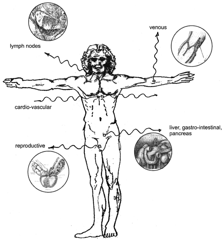 Applications include in vivo flow cytometry and ex vivo dermal contact cytometry of blood. Internally implanted devices might be coupled with molecular recognition sensors to trigger optical readout through transparent tissue. The light beams would be intense, and exhibit much light scattering, so it is preferable to locate them close to the dermis. Issues arise about how to anchor them in place and avoid migration in the body, or how to supply power (implanted battery, rf coupling). It is even possible to consider using the material as an internal power source by coupling external light into a photovoltaic junction. It may be possible to include both photovoltaic and photo-emitting action in the same implanted microdevice. In each of these cases, biocompatibility becomes a major consideration and it is necessary to determine if the materials induce harmful effects when they are in intimate contact with living cells. Some of the possible negative effects may include activation of an immune response, hemolysis, gene mutation, carcinogenicity, tumorogenicity, inhibition of cell growth, irritation, and toxicity. This thrust represents the advent of a fertile new uncharted area of research that interfaces between materials science and living systems at the micro- and nanoscale levels. Biocompatibility of micro- and nanostructured materials would need to be studied in some detail from both the materials and biological perspectives to discover ways in which to mitigate detrimental responses of the body to foreign atomic species. Much of the initial research would be done in vitro with cell cultures to understand the basic mechanisms of cytotoxicity and genotoxicity. Questions arise as to the type and form of atomic/ionic/molecular species that detach from material surfaces and become incorporated into the cell membrane, nucleus, cytoplasm, or organelles and destabilize the metabolic cycle. On the biological side, research might develop new assays of chromosomal aberration to assess the impact of atomic/ionic/molecular species. Other issues that arise from the biological perspective are carcinogenicity, the role of bacterial endotoxins from material surfaces, and hemocompatibility including material effects on coagulation, hemolysis, and thrombosis. Ex vivo dermal contact materials would stimulate the need to study irritation and acute toxicity. As this field develops, implantation studies in suitable animal species would unfold additional domains of material biocompatibility. AcknowledgmentsThe authors are grateful to Dr. L. Sklar of the University of New Mexico Cancer Center for use of cell growth facilities and to Charles A. Evans and Associates for performing the SIMs analysis. This work was supported under DOE Contract No. DE-AC04-94AL85000 and the Office of Basic Energy Sciences. REFERENCES
P. L. Gourley
,
A. E. McDonald
,
J. K. Hendricks
,
G. C. Copeland
,
J. Hunter
,
O. Akhil
,
J. L. Dunne
,
S. L. Skirboll
,
L. Nihlen
, and
H. J. Capps
,
“Nanolaser/microfluidic biochip for realtime tumor pathology,”
J. Biomed. Microdevices , 2 111
–122
(2000). Google Scholar
P. L. Gourley
,
O. Akhil
,
G. C. Copeland
,
J. L. Dunne
,
J. K. Hendricks
,
A. E. McDonald
,
S. L. Skirboll
, and
L. Nihlen
,
“A semiconductor microlaser for intracavity flow cytometry,”
Proc. SPIE , 3606 64
–73
(1999). Google Scholar
V. V. Tuchin
,
“Lasers and fiber optics in medicine,”
Proc. SPIE , 1981 2
–16
(1992). Google Scholar
P. L. Gourley
and
D. Y. Sasaki
,
“Biocavity lasers,”
Am. Sci. , 89 152
–159
(2001). Google Scholar
P. L. Gourley
and
M. F. Gourley
,
“Biocavity lasers for biomedicine,”
Trends Biotechnol. , 18 443
–448
(2001). Google Scholar
P. L. Gourley
,
J. D. Cox
,
J. K. Hendricks
,
A. E. McDonald
,
R. G. Copeland
,
D. Y. Sasaki
,
M. Curry
and
S. L. Skirboll
,
“Semiconductor microcavity laser spectroscopy of intracellular protein in human cancer cells,”
Proc. SPIE , 4265 113
–124
(2001). Google Scholar
G. Kotzar
,
M. Freas
,
P. Able
,
A. Fleischman
,
S. Roy
,
C. Zorman
,
J. M. Moran
, and
J. Melzak
,
“Evaluation of MEMS material of construction for implantable medical devices,”
Biomaterials , 23 2737
–2750
(2002). Google Scholar
H. Mammerle
,
K. Kobuch
,
K. Kohler
,
W. Nisch
,
H. Sachs
, and
M. Stelzle
,
“Biostability of micro-photodiode arrays for subretinal implantation,”
Biomaterials , 23 797
–804
(2002). Google Scholar
J. D. Cox
,
M. S. Curry
,
S. K. Skirboll
,
P. L. Gourley
, and
D. Y. Sasaki
,
“Surface passivation of a microfluidic device to glial cell adhesion: A comparison of hydrophobic and hydrophilic SAM coatings,”
Biomaterials , 23 929
–935
(2002). Google Scholar
D. Y. Sasaki
,
J. Cox
,
S. C. Follstaedt
,
M. S. Curry
,
S. K. Skirboll
, and
P. L. Gourley
,
“Glial cell adhesion and protein adsorption on SAM-coated semiconductor and glass surfaces,”
Proc. SPIE , 4265 152
–163
(2001). Google Scholar
M. Altosaar
and
P.-E. Kukk
,
“Radiative and nonradiative recombination centers in Cl and Na doped CdTe monograin powders,”
J. Mater. Sci. , 35 11358
(2000). Google Scholar
M. Grun
,
A. Storzum
,
M. Hetterich
,
A. Kamilli
,
W. Send
,
T. Walter
, and
C. Klingshirn
,
“Chlorine doping of cubic CdS and ZnS grown by compound source molecular-beam epitaxy,”
J. Cryst. Growth , 201–202 457
–460
(1999). Google Scholar
B. Roling
,
C. Martiny
, and
S. Bruckner
,
“Ion transport in glass: Influence of glassy structure on spatial extent of nonrandom ion hopping,”
Phys. Rev. B , 63
(21), 214203
–214219
(2001). Google Scholar
|


CITATIONS
Cited by 7 scholarly publications.
Semiconductors
Ions
Interfaces
Sodium
Semiconducting wafers
Compound semiconductors
Molecules


