
|
|
1.IntroductionElastic light scattering has the potential of serving as a label-free, noninvasive approach for revealing the rich morphological and biological information about cells.1, 2 A growing number of noninvasive optical diagnostics techniques such as optical coherence tomography3 and light scattering spectroscopy4, 5 require a fundamental understanding of light scattering from single biological cells. When polarized laser light illuminates a cell, the spatial distribution of the scattered light is not random and is dependent on the detailed cell structure. For example, the nucleus, which is the largest organelle in a cell, is the main contributor to scattered light at small angles.1, 6 Numerous studies indicate that nanoscale structures such as mitochondria within a cell play an important role in the side scatter. 1, 2, 6, 7, 8 The ability to obtain and analyze scattered light at different angular ranges or over a wide angular range is therefore potentially important for cellular analysis. The development of miniaturized cytometers9, 10 with the potential to measure scattered light over a broad 2D angular range10 has recently been reported. The task of obtaining side-scatter patterns is challenging due to the lower intensity level of the side-scattered light and the difficulty in resolving the angular structure of this scattering. A further problem concerns single cell scattering where researchers have resorted to short integration times in order to obtain light spectra in a fluidic flow.11 However, short integration times require high-quality detectors and high-power lasers. Furthermore, the validation of a particular light scattering measurement approach requires that comparisons be made with theoretical models such as Mie theory12, 13 or by using numerical simulations such as the finite-difference time-domain (FDTD) method. 2, 8, 14, 15 This is not easily accomplished when complex experimental setups are involved. In the recent study by Yu, 16 2D scattered light spectra have been used to differentiate between healthy and cancerous colon tissue. The cancerous tissue exhibited much greater asymmetry in the azimuthal dependence of the scattered pattern than the healthy tissue. In this study we describe and validate a compact planar waveguide cytometer that is capable of obtaining 2D side-scatter patterns. The reported system addresses a number of issues such as the resolution of the angular dependence of the scattering, the issue of short integration times, and the ability to compare experimental results with known theoretical predictions. The absence of an optical lens in this planar waveguide structure allows a resolution of the angular dependence of the scattering to be made as well as simplifies the comparison of measured results with predictions obtained using either Mie theory or simulations employing the FDTD method. The single scatterer can be immobilized in the observation window area in the microchip by pressure control, which makes a longer integration time for the light scattering measurements practical. The 2D features of the scatter patterns (symmetrical about the azimuth angle ) are used to develop a method for determining the location of 90-deg scatter. The operation of this cytometer is validated in this study through the use of polystyrene microbeads in the microfluidic channel. Comparisons of the 2D scatter patterns that are experimentally obtained with Mie theory predictions confirm the correct operation of the device. A Fourier method for size differentiation of the scatterers has also been developed. This is based on comparisons between the Fourier peaks of Mie theory simulations and experimental results from polystyrene beads that range in size from 4 to . In a separate publication,17 our new cytometer was used in a qualitative study of 2D scattered light spectra from yeast and Raji cells. Scattering from the randomly distributed mitochondria in Raji cells has been identified as the cause of small-scale 2D structures in the scattered light pattern. This is in contrast with the light scattering patterns from yeast cells, which show clear fringes very similar to angular spectra from beads considered here. As an integrated biomedical optics instrument, our 2D cytometer has an important potential application in biological cell diagnostics. In this paper, a detailed description of the instrument is given including the wave propagation in a liquid-core waveguide. We have developed the quantitative Fourier-transform-based method of size determination of polystyrene beads and calibrated the cytometer. Clearly this method could be very efficient in finding out the size of scattering objects, cells or beads, if the Fourier transform of the scattered light angular distribution contains a dominant peak with a finite frequency. This is the case for biological cells without internal structure, for example, isovolumetrically sphered red blood cells.18 Alternatively, one could consider cells with one large-sized organelle that has the largest scattering cross section, such as a nucleus with a large index of refraction, as for example in stem cells. 2.Experimental and Simulation Methods2.1.Microchip FabricationIn order to improve the signal-to-noise ratio of our cytometer, an aluminum-coated glass slide with etched observation windows was fabricated [see substrate in Fig. 1a ]. The thin aluminum film will block most of the noise (scattering from the scatterers not in the observation window and from the microfluidic channel structure) from being collected by the detector. To fabricate the aluminum-coated glass slide, aluminum was sputtered onto a Borofloat glass substrate (Paragon Optical Co., Reading, PA, USA) by using a magnetron sputtering system (Kurt J. Lesker Co., Clairton, PA, USA). The coated aluminum thickness measured by using an Alpha-step 200 contact profilometer (KLA-Tencor, San Jose, CA, USA) is . Optical simulations using the transfer matrix technique19, 20 show that an aluminum film (refractive index ) with a thickness of will block 99% of the incident light (wavelength ) from water (refractive index 1.334) to glass (refractive index 1.47) at an incident angle of . A thin photoresist coating (Shipley Microelectronics, Marlboro, MA, USA) was then spun onto the film sides of the substrates. The photomask used was printed on a transparency film (Fuji Luxel V-9600 CTP, Fuji Photo Film Co., Japan). After UV exposure, the substrates were developed by using the Shipley 354 developer and etched with Al etchant (Arch Chemicals Inc., Norwalk, CT, USA). Fig. 1(a) Microchip fabrication using UV epoxy edge bonding and (b) the integrated experimental setup. In (a), the superstrate is a standard glass slide. The middle layer is a polymer sheet with a cut-out channel, and the substrate is an aluminum-coated glass slide with etched microsized observation windows. The inset shows the microchip used in this experiment. In (b), the CCD array used to capture the scatter patterns is placed in an aluminum box. The CCD array is connected to a computer to record the data. The digital camera that is used to image the beads in the channel is mounted on top of the microscope.  A method that combines the standard gasket method21 and the epoxy method22 for microfluidic chip fabrication was used and is illustrated in Fig. 1a. 2.2.Integration of the Microfluidic Waveguide SystemFigure 1b shows the experimental system. The laser is mounted on an optical bread board and its orientation with respect to the microchannel can be adjusted in order to set the angle of incidence [see Fig. 2a ]. In this study, a linearly polarized laser (Melles Griot, Ottawa, ON, Canada) with a wavelength of and a maximum power of is used as the illumination source. The laser beam is coupled into the channel via a BK7 prism (Edmund Industrial Optics, Barrington, NJ, USA). A 2D CCD array (ICX098BQ, Sony, Japan) is placed in close proximity to the chip directly under one of the etched observation windows. An 8-bit analog/digital converter is used with the CCD. The CCD has a chip size of approximately and effective pixels. The experimental setup is depicted in Fig. 2a. The core part of the integrated waveguide system is a compact structure, including the prism, microchip, and the CCD detector. The waveguide used here is known as a leaky waveguide10, 23 Compared with the well-known prism coupling method reported by Tien,24 which uses an evanescent light coupling in the thin film, we take advantage of the leaky nature of our system to excite a leaky optical mode in the channel. The laser light is incident on the microchip at the phase matching angle25 (in our case, the phase matching angle is approximately ), and the optical mode or modes in the waveguide propagate along the microchannel. Once a scatterer is immobilized in the observation window area, a frame of the 2D scattered light pattern is taken by using the CCD (integration time ) that is located beneath the microchannel. A defocused scatter pattern image is also taken by using a digital camera (Nikon Coolpix 990, Nikon Corp., Japan) that is mounted on top of the microscope. The integration time used is (F4). Fig. 2(a) Schematic cross section of the experimental setup shown in Fig. 1b and (b) the planar waveguide structure used in this experiment [corresponding to the circled area in (a)]. In (a), the laser light is coupled into the channel by using the prism that is located on the microchip. The arrows show the laser mode propagation direction. The CCD is beneath the microchip with the observation window projected to the center of the CCD screen field. In (b), the dimensions of this structure are approximately . The laser is assumed to propagate in the direction. The scattered light was projected onto the CCD screen as shown by the arrows. 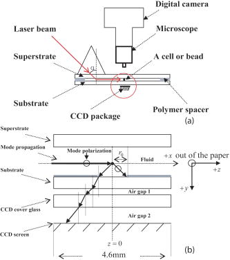 2.3.Mapping the Mie Simulation Results onto the Planar CCDThe microfluidic chip [Fig. 2b] used in this study has a channel height of , which supports multimode propagation in the waveguide. The transfer matrix method was used to determine the propagation modes for the planar waveguide.19, 20 Different modes are excited because of the laser divergence. By taking into account the Gaussian distribution of the laser intensity and the coupling coefficients for the laser light to excite a given mode, the mode profiles for the order, order, and order modes are shown in Fig. 3 . The summation of the first 21 modes supported by the waveguide structure is shown in Fig. 3 as the dark solid line. Higher order modes are not excited due to the small laser divergence . This summed mode profile has a uniform intensity distribution across the waveguide intersection except very close to the substrate, while most beads will travel in the uniformly distributed intensity area. Second, the incident laser light is polarized along the -direction before it is coupled into the waveguide. Thus only the TE mode (polarized along the axis) is excited in the planar waveguide. This mode will retain its polarization (the loss of polarization due to the stress-induced birefringence is negligible in our liquid-core waveguide) for the propagation along all values of in the linear isotropic medium that is used here (water).26 In a ray diagram representation of mode propagation in a waveguide, the propagation direction of the distinct modes can be regarded as a zig-zag pattern.24 In a thick waveguide such as the one considered , all modes are almost paraxial. Thus all modes can be assumed to be propagating in a direction parallel to the axis and there is no divergence due to the mode propagation through the waveguide. Based on the above analysis, an assumption is made that the bead is illuminated by a plane wave. In this case, Mie theory can be used for describing light scattering from a microsized bead in the integrated waveguide cytometer. Fig. 3Mode profiles in the microfluidic waveguide. The dark line shows the summation of the first 21 modes from order to order. The dotted line is for the order mode, the cross signs are for the order mode, and the circle signs are for the order mode.  Scatter patterns from the polystyrene beads (which are assumed to be spherical and homogeneous) are studied in this report. Mie theory gives exact solutions for the scatter patterns from these ideal scatterers. For an incident laser propagating in the direction as shown in Fig. 2b, Mie theory gives the spatial scattered intensity distribution (at a certain distance) as a function of polar angle and azimuth angle . The angle is measured from the axis, and the azimuth angle in the plane. The mode polarization in the waveguide is the same as the scattered light polarization.12 To compare Mie simulations with the observed experimental results, it is necessary to map the calculated far-field scattering pattern onto the CCD screen. Figure 2b shows the integrated planar waveguide structure. The planar structure simplifies the ray tracing procedure for the propagation of the scattered light in the system. Another advantage of this system is that there are no optical lens systems between the CCD detector and the scatterer in the channel. This dramatically simplifies the comparisons between the experimental results and the Mie simulation results. A code has been developed for projecting the Mie theory spatially distributed scattered intensity onto the CCD screen, and Snell’s law has been used for the multilayer ray trace as shown in Fig. 2b. At each interface, the Fresnel equations are applied for intensity transfer. In the current experiments, the range of the scatter angle is determined by the height of the microchannel relative to the diameter of the observation window, the CCD effective screen size, and the integrated waveguide structure as shown in Fig. 2b. We assume that the bead is away from the glass substrate (refractive index 1.47, in thickness). The air gap 1 between the CCD detector and the microchip is in thickness. The cover glass thickness of the CCD detector is (refractive index 1.5), and the distance between the cover glass and the CCD sensor is —air gap 2. Such configurations allow the detection of the scatter angle in the angular range approximately if the scatterer is centered right above the CCD center. As in Fig. 4 , we give the sample calculation results for a polystyrene bead (refractive index 1.591) at as shown in Fig. 2b in a surrounding medium of water (refractive index 1.334). The illumination laser wavelength is , and polarized along the axis. Figure 4a shows the perpendicular polarization light scattering intensity distribution on the CCD screen versus the scatter angle . Figure 4b gives the relationship between the CCD position and the scatter angle. The relationship between the scatter angle and the CCD position is not linear, and this relationship is determined by the integrated waveguide structure—it is the same for all the polystyrene beads used in this study. From Fig. 4b, an angular resolution of approximately (420 pixels in the angular range ) for the light scattering measurements can be achieved in our integrated waveguide cytometer. Figure 4 shows the scattering angular range that will only be considered in detail in the following study from 61 to , which corresponds to approximately on the CCD [90-deg scatter corresponds to a position at as shown in Fig. 4b]. Fig. 4Mie simulation results for scattering from a polystyrene bead onto the CCD screen: (a) angular distribution of the scattered intensity from a polystyrene bead onto the CCD screen and (b) the correlation between the position on CCD and the scatter polar angle for the integrated waveguide structure used in this report.  3.Results and Discussion3.1.Determining the Location of 90-deg Scatter in the Scatter PatternsThe polystyrene beads used in this study included 4- and -diameter (Interfacial Dynamics Corp., Tualatin, OR, USA), and 15- and diameter (Fluka, Sigma-Aldrich, St. Louis, MO, USA) beads. The beads were in suspension in filtered water ( filter, Millipore Corp., Billerica, MA, USA), and were diluted to a concentration of and sonicated for . The well-diluted bead solution made single bead observations in the observation window area possible. The solution was then pumped into the channel which was prefilled with filtered water by using a syringe pump. Once the system was well aligned (ideally, the observation is projected right onto the center of the CCD although experimentally there might be an offset of several hundred microns), we focused the microscope on the observation window [ in diameter as shown in Fig. 1a]. Positive pressure was applied to induce flow along the direction until a single scatterer was seen in the observation window. Reverse pressure was applied to immobilize the single scatterer in the observation window area as required. Knowledge of the scatterer position relative to the detector enables one to determine whether the scattered light intensity distribution corresponds to forward, side, or backward scattering. After positioning a microbead in the observation window using the digital camera mounted on top of the microscope, 2D scatter patterns were taken by using the CCD detector located beneath the microchip. Experimental background frames are obtained when there is no microbead in the observation window area. The experimental background frame is clear of any fringes, thereby showing that any multiple reflections in the layered structure have a negligible effect on the peak numbers and the peak positions of the scatter patterns obtained. As shown in Figs. 5a and 5b , the arrow indicates the direction of the mode propagation, which is the same direction as the flow in the channel. Note that the flow and mode propagation directions obtained from the camera [Figs. 5a and 5b] are opposite to those obtained from the CCD [Figs. 5a ′ and 5b ′]. As the bead entered the observation window area from right to left, the defocused scatter images as shown in Figs. 5a and 5b were obtained. The scatter patterns as shown in Figs. 5a ′ and 5b ′ were obtained by using the CCD beneath the microchip. If a 2D ray trace is performed, 90-deg scatter will give vertical fringes. The forward scatter gives hyperbolic fringes open to the direction , while the backward scatter gives hyperbolic fringes open to the direction . These features are shown in Figs. 5a ′ and 5b ′. While the defocused image shows the bead at the right side as in Fig. 5b; its 90-deg scatter for the high-resolution scatter pattern in Fig. 5b ′ is centered to the left side of the CCD frame. The defocused image shows the bead at the left side as in Fig. 5a; its 90-deg scatter for the high-resolution scatter pattern in Fig. 5a ′ is centered to the right side of the frame. As in Fig. 5a ′, the 90-deg scatter is centered about pixel column position 340, while in Fig. 5b ′, the 90-deg scatter is centered about pixel column position 290. Since the size of the CCD is horizontally and the frame has 640 pixels, this 50-pixel difference corresponds to a distance of , which is approximately the distance (the observation window diameter) that the bead has traveled from Fig. 5b to Fig. 5a. In the analysis that follows, the 90-deg scatter location in the 2D scatter patterns is determined by using the above method. Fig. 5Identifying the location of 90-deg scattering in our system. (a) and (b) are the defocused scatter images obtained from a digital camera mounted on the top of the microscope, and and are the 2D scatter patterns obtained from the CCD beneath the microchip. The arrows show the direction of waveguide mode propagation. The circles indicate the 90-deg scatter locations.  3.2.Size Differentiation of Polystyrene Microbeads3.2.1.Wide-angle comparisons of light scattering patternsFigures 6a to 6d are the defocused scatter images taken by using a digital camera for different-sized polystyrene beads. Clear fringes are obtained, which show that the bead is stationary over a time period of . For the defocused scatter patterns shown in Fig. 6, the bigger the scatterer size, the greater are the numbers of the fringes detected. This information helps one to infer the size of the bead in the fluidic flow. The high-resolution 2D scatter patterns obtained by using a CCD array for polystyrene beads for sizes ranging from 4 to are shown in Figs. 6a ′, 6b ′, 6c ′, and 6d ′. We refer to high-resolution images as those with a greater number of observable fringes as compared with the defocused scatter images. These high-resolution 2D scatter patterns contain more information about the scatterers as compared with the 1D scatter spectra obtained in light scattering measurements. In this report, we only explore the 2D features to determine the position for 90-deg polar angle scatter and the position for an azimuth angle . However, we believe that the 2D scatter patterns can be used to provide a better understanding of the light scattering problems involving single biological cells. Fig. 6(a), (b), (c), and (d) Defocused scatter images for 4-, 9.6-, 15-, and beads, respectively. The dark circular area in (a), (b), (c), and (d) is the observation window under the microscope. 2D high-resolution scatter patterns are shown in 4 to for the 4-, 9.6-, 15-, and beads, respectively.  In order to compare the experimental results and Mie simulation results, experimental scatter patterns in Figs. 6a ′, 6b ′, 6c ′, and 6d ′ are scanned for 420 pixels horizontally (angular range , determined by the 90-deg scatter method), and averaged over 3 pixels vertically (pixel 239 to pixel 241). Pixel (0, 0) is at the upper left corner, and pixel (419, 479) is at the lower right corner. Following the ray tracing procedure depicted in Fig. 2b, the 2D scatter pattern of a bead obtained from the CCD will be symmetrical about the azimuth angle . This property is exhibited by the experimental results in Figs. 6a ′, 6b ′, 6c ′, and 6d ′. Thus the vertically averaged results from pixel 239 to pixel 241 give the scatter intensity distribution around the azimuth angle . As the waveguide mode is polarized in the direction [shown in Fig. 2b], the scan of the experimental scatter pattern gives the perpendicular polarization scatter results. Wide-angle comparisons between Mie simulation results and the experimental results are now given in the space domain. Figures 7a and 7b show the representative comparisons in the space domain for 9.6- and beads [Figs. 6b ′ and 6c ′], respectively. We obtained 13 peaks for beads and 19 peaks for beads both from Mie theory simulations and from experimental results. The peak locations match well between Mie simulation results and experimental results for both the and the beads, especially in the position range , which is in the angular range of [according to Fig. 4b]. We apply a Fourier high-bandpass filter 0.5 (1/mm) on the experimental results in Figs. 7a and 7b. The filtered experimental results are shown in Figs. 7a and 7b as solid lines, which show that the experimental bumps can be removed by filtering out smallest frequency components in the Fourier domain. The filtered experimental results give better comparisons with the Mie simulation results. The good agreements between the peak numbers and peak positions in the experimental and theoretical spectra for both and beads demonstrated in Figs. 7a and 7b also confirm the effectiveness of our method for determining the location of scatter in the 2D scatter patterns. Fig. 7Wide-angle comparisons between experimental and Mie simulation results. (a) and (b) show the wide-angle comparisons between Mie simulation and experimental results. The dotted line shows the Mie simulation results, and the solid line with plus signs shows the experimental results. (c) and (d) show the comparisons in the Fourier domain for both 9.6- and bead results. The Fourier spectra are normalized to have typical peak amplitudes of 1.5 and 1.0 for the Mie simulation and experimental results, respectively.  Because the angular intensity distribution of the Mie results for any scatterer has an oscillatory distribution,18 we explore the application of Fourier transforms on both the Mie simulation results and the experimental results and perform wide-angle comparisons in Fourier domain. Figures 7c and 7d show the representative comparisons in the Fourier domain for both 9.6- and beads [frequency components greater than 20 (1/mm) are with very small amplitudes and not shown here], respectively. The typical peak for the experimental result was determined as the highest frequency peak from the dominant part of the full Fourier spectra. As there is no single scatterer in the medium that is larger than the bead, the amplitudes of the frequency components beyond this typical peak are significantly smaller. The comparisons show that the bead has a typical peak located at 4.1 (1/mm) both from Mie simulations and experimental results, and 6.2 (1/mm) for the bead. In Fig. 7, the Fourier transforms of the Mie simulation results give only one dominant peak over the whole Fourier spectrum for each bead size. Thus the bead sizes can be estimated by the locations of this dominant peak. These typical peak positions [Figs. 7c and 7d] in the Fourier domain correspond to the frequency of intensity oscillations [Figs. 7a and 7b] in the space domain, and increase with the particle sizes. The use of the frequency of oscillations in the intensity of scattered light to assess size has also been demonstrated by Canpolat and Mourant.27 In Figs. 7c and 7d, good agreements are obtained for the typical peak positions between the Mie theory and experimental results in the Fourier domain. 3.2.2.Fourier analysis for size differentiationThe above study shows that the oscillatory property of the scattered intensity distribution will give certain peaks in the frequency domain. Applying this principle for beads ranging from 4 to in diameter, a Fourier method for size differentiation is developed. Peak-by-peak comparisons in the spatial domain are complicated by nonuniform intensity variations resulting from the geometrical projection, losses, and background noise. The above analysis shows that a Fourier analysis can be used to extract the frequency components from the scattered signals despite the experimental background that is present in our current experiments. Note that intensity variations cannot change the locations of the Fourier peaks. This size differentiation method has advantages over the normal optical microscopy for spherical particle size differentiation, as a normal optical microscope requires a rigid focus and is not suitable for performing measurements on objects in fluidic flow. The Fourier method developed here can potentially be useful for the real-time characterization of cell samples in clinics. The Fourier transform was applied to all the Mie simulations and the experimental results for the polystyrene beads ranging in size 4 to . In Fig. 8 , the open squares and triangles indicate the Fourier results for the Mie simulations of the beads with an air gap 1 [see Fig. 2b] of thickness 350 and , respectively. The cross signs are the Fourier results for the experimental patterns as shown in Fig. 6. Referring back to Fig. 2b, the thicknesses of air gap 1 and air gap 2 play important roles as the light travels from an optically dense medium into air. As shown in Fig. 8, an air gap thickness of gives higher frequency peak position values as compared with an air gap thickness of . In both cases, the correlation between the Fourier peak position and the bead size is linear. Fig. 8FFT method for microsized differentiation. Fourier peaks of the experimental and Mie simulation results for 4-, 9.6-, 15-, and beads are shown. The open squares and triangles are the Mie simulation results for the four different sizes of beads, for an air gap 1 thickness of 350 and , respectively. Fourier peaks of four different sets of the experimental results are shown; each set includes 4-, 9.6-, 15-, and beads.  A Fourier analysis was also performed on different sets of experimental results. Each set of the experimental results includes 4-, 9.6-, 15-, and beads. The Fourier peak positions of the other three sets of experimental scatter patterns are denoted as plus signs, open circles, and solid dots in Fig. 8. The 512-point Fourier transform that has been used has a resolution of approximately 0.27 in frequency (1/mm), which gives an uncertainty of approximately for the size estimations [from Figs. 7c and 7d]. The Fourier peaks of the experimental results shown in Fig. 8 fall within this uncertainty range. The solid line in Fig. 8 is a linear regression of all the experimental results. This linear curve can be used to perform size calibrations independent of Mie theory. Despite differences that result from the air gap 1 thickness, Fig. 8 shows the effectiveness of the Fourier method for size differentiation. The Fourier transform method that is developed here can be used for measuring particles as small as or even smaller by using a shorter incident wavelength illumination with a wider angle of observation. We have performed Mie theory simulations of 750- and 1500-nm polystyrene beads with the same layer thicknesses and material as in the present study but over a wider angular range of , with a short laser illumination wavelength of . A Fourier analysis of these spectra shows that the 750-nm bead has a sharp typical peak at 0.42 (1/mm), while that of the 1500-nm is at 1.05 (1/mm), with a resolution of 0.105 in frequency (1/mm). Even with the current restricted angular range of , we have measured several scatter fringes of a bead [Fig. 6a ′], which lead to a well-defined peak in the Fourier spectrum. As long as we can identify several such intensity maxima, which correspond to a submicron-sized bead in the current geometry, our method will work. Future improvements that include a wider angle observation with an illumination source that has a shorter wavelength would improve the resolution of the spectral method below the current limit to particle sizes of several hundred nanometers. As discussed above, the Fourier transform analysis of the light scattering in the angular range has a frequency resolution of 0.105 (1/mm), which corresponds to a resolution of for size differentiation. This higher resolution can be used to study the distributed cell and organelle sizes. The calibration curve of Fig. 8 can be applied in size determination of scatterers of arbitrary size provided a characteristic peak can be identified in the Fourier spectrum. 4.ConclusionsAn integrated microfluidic waveguide cytometer that is capable of obtaining high-resolution 2D side-scatter patterns has been introduced in this paper. The obtained 2D scatter patterns together with the no-lens planar optical design ensure a better resolution of the angular dependence of the side-scatter spectra. The use of Mie theory or simulation methods such as the FDTD to validate the experimental results are dramatically simplified when such an integrated structure is used. A Fourier method was developed for size differentiation of homogeneous spherical scatterers. The analysis is confirmed by Mie theory simulations of scattering from the polystyrene beads used in the experiment. Currently, the experimental setup is capable of observing only side-scattered light. Interestingly, this angular region has been shown in previous studies to be particularly sensitive to the affects of nanoscale particles such as organelles within biological cells, as was demonstrated in a publication of 2D light scattering patterns from Raji cells.17 AcknowledgmentsThe authors thank NanoFab (University of Alberta, Canada) for supporting the fabrication of the microchips. This work is supported by the Natural Science and Engineering Research Council (NSERC) of Canada. ReferencesJ. R. Mourant,
J. P. Freyer,
A. H. Hielscher,
A. A. Eick,
D. Shen, and
T. M. Johnson,
“Mechanisms of light scattering from biological cells relevant to noninvasive optical-tissue diagnostics,”
Appl. Opt., 37
(16), 3586
–3593
(1998). 0003-6935 Google Scholar
C. G. Liu,
C. Capjack, and
W. Rozmus,
“3-D simulation of light scattering from biological cells and cell differentiation,”
J. Biomed. Opt., 10
(1), 014007
(2005). https://doi.org/10.1117/1.1854681 1083-3668 Google Scholar
G. J. Tearney,
M. E. Brezinski,
B. E. Bouma,
S. A. Boppart,
C. Pitris,
J. F. Southern, and
J. G. Fujimoto,
“In vivo endoscopic optical biopsy with optical coherence tomography,”
Science, 276
(5321), 2037
–2039
(1997). https://doi.org/10.1126/science.276.5321.2037 0036-8075 Google Scholar
V. Backman,
M. B. Wallace,
L. T. Perelman,
J. T. Arendt,
R. Gurjar,
M. G. Muller,
Q. Zhang,
G. Zonios,
E. Kline,
T. McGillican,
S. Shapshay,
T. Valdez,
K. Badizadegan,
J. M. Crawford,
M. Fitzmaurice,
S. Kabani,
H. S. Levin,
M. Seiler,
R. R. Dasari,
I. Itzkan,
J. Van Dam, and
M. S. Feld,
“Detection of preinvasive cancer cells,”
Nature (London), 406
(6791), 35
–36
(2000). https://doi.org/10.1038/35017638 0028-0836 Google Scholar
I. J. Bigio,
S. G. Bown,
G. Briggs,
C. Kelley,
S. Lakhani,
D. Pickard,
P. M. Ripley,
I. G. Rose, and
C. Saunders,
“Diagnosis of breast cancer using elastic-scattering spectroscopy: preliminary clinical results,”
J. Biomed. Opt., 5
(2), 221
–228
(2000). https://doi.org/10.1117/1.429990 1083-3668 Google Scholar
H. B. Steen and
T. Lindmo,
“Differential of light-scattering detection in an arc-lamp-based epi-illumination flow cytometer,”
Cytometry, 6
(4), 281
–285
(1985). https://doi.org/10.1002/cyto.990060402 0196-4763 Google Scholar
J. D. Wilson,
C. E. Bigelow,
D. J. Calkins, and
T. H. Foster,
“Light-scattering from intact cells reports oxidative-stress-induced mitochondrial swelling,”
Biophys. J., 88
(4), 2929
–2938
(2005). https://doi.org/10.1529/biophysj.104.054528 0006-3495 Google Scholar
A. Dunn and
R. Richards-Kortum,
“Three-dimensional computation of lightscattering from cells,”
IEEE J. Sel. Top. Quantum Electron., 2
(4), 898
–905
(1996). https://doi.org/10.1109/2944.577313 1077-260X Google Scholar
Z. Wang,
J. El-Ali,
M. Engelund,
T. Gotsaed,
I. R. Perch-Nielsen,
K. B. Mogensen,
D. Snakenborg,
J. P. Kutter, and
A. Wolff,
“Measurements of scattered light on a microchip flow cytometer with integrated polymer based optical elements,”
Lab Chip, 4
(4), 372
–377
(2004). https://doi.org/10.1039/b400663a 1473-0197 Google Scholar
K. Singh,
X. T. Su,
C. G. Liu,
C. Capjack,
W. Rozmus, and
C. J. Backhouse,
“A miniaturized wide-angle 2D cytometer,”
Cytom. Part A, 69A
(4), 307
–315
(2006). Google Scholar
J. Neukammer,
C. Gohlke,
A. Hope,
T. Wessel, and
H. Rinneberg,
“Angular distribution of light scattered by single biological cells and oriented particle agglomerates,”
Appl. Opt., 42
(31), 6388
–6397
(2003). https://doi.org/10.1364/AO.42.006388 0003-6935 Google Scholar
W. T. Grandy, Scattering of Waves from Large Spheres,
(2000) Google Scholar
G. Mie,
“Articles on the optical characteristics of turbid tubes, especially colloidal metal solutions,”
Ann. Phys.-Berlin, 25
(3), 377
–445
(1908). Google Scholar
R. Drezek,
A. Dunn, and
R. Richards-Kortum,
“A pulsed finite-differencetime-domain (FDTD) method for calculating light scattering from biological cells over broad wavelength ranges,”
Opt. Express, 6
(7), 147
–157
(2000). 1094-4087 Google Scholar
J. Q. Lu,
P. Yang, and
X. H. Hu,
“Simulations of light scattering from a biconcave red blood cell using the finite-difference time-domain method,”
J. Biomed. Opt., 10
(2), 024022
(2005). https://doi.org/10.1117/1.1897397 1083-3668 Google Scholar
C. C. Yu,
C. Lau,
J. W. Tunnell,
M. Hunter,
M. Kalashnikov, and
C. Fang-Yen,
“Assessing epithelial cell nuclear morphology by using azimuthal light scattering spectroscopy,”
Opt. Lett., 31
(21), 3119
–3121
(2006). https://doi.org/10.1364/OL.31.003119 0146-9592 Google Scholar
X. T. Su,
C. Capjack,
W. Rozmus, and
C. Backhouse,
“2D light scattering patterns of mitochondria in single cells,”
Opt. Express, 15
(17), 10562
–10575
(2007). https://doi.org/10.1364/OE.15.010562 1094-4087 Google Scholar
N. Ghosh,
P. Buddhiwant,
A. Uppal,
S. K. Majumder,
H. S. Patel, and
P. K. Gupta,
“Simultaneous determination of size and refractive index of red blood cells by light scattering measurements,”
Appl. Phys. Lett., 88
(8), 084101
(2006). https://doi.org/10.1063/1.2176854 0003-6951 Google Scholar
R. T. Kersten,
“Prism-film coupler as a precision instrument. 1. Accuracy and capabilities of prism couplers as instruments,”
Opt. Acta, 22
(6), 503
–513
(1975). 0030-3909 Google Scholar
J. Petráček and
K. Singh,
“Determination of leaky modes in planar multilayer waveguides,”
IEEE Photonics Technol. Lett., 14
(6), 810
–812
(2002). https://doi.org/10.1109/LPT.2002.1003101 1041-1135 Google Scholar
L. Licklider,
X. Q. Wang,
A. Desai,
Y. C. Tai, and
T. D. Lee,
“A micromachined chip-based electrospray source for mass spectrometry,”
Anal. Chem., 72
(2), 367
–375
(2000). https://doi.org/10.1021/ac990967p 0003-2700 Google Scholar
P. Sethu and
C. H. Mastrangelo,
“Cast epoxy-based microfluidic systems and their application in biotechnology,”
Sens. Actuators B, 98
(2–3), 337
–346
(2004). 0925-4005 Google Scholar
R. T. Kersten,
“Prism-film coupler as a precision instrument. 2. Measurements of refractive-index and thickness of leaky waveguides,”
Opt. Acta, 22
(6), 515
–521
(1975). 0030-3909 Google Scholar
P. K. Tien,
“Light waves in thin films and integrated optics,”
Appl. Opt., 10
(11), 2395
–2413
(1971). 0003-6935 Google Scholar
N. J. Harrick, Internal Reflection Spectroscopy, Wiley, New York (1967). Google Scholar
I. P. Kaminow,
“Polarization in optical fibers,”
IEEE J. Quantum Electron., 17
(1), 15
–22
(1981). https://doi.org/10.1109/JQE.1981.1070626 0018-9197 Google Scholar
M. Canpolat and
J. R. Mourant,
“Particle size analysis of turbid media with a single optical fiber in contact with the medium to deliver and detect white light,”
Appl. Opt., 40
(22), 3792
–3799
(2001). https://doi.org/10.1364/AO.40.003792 0003-6935 Google Scholar
|


