|
|
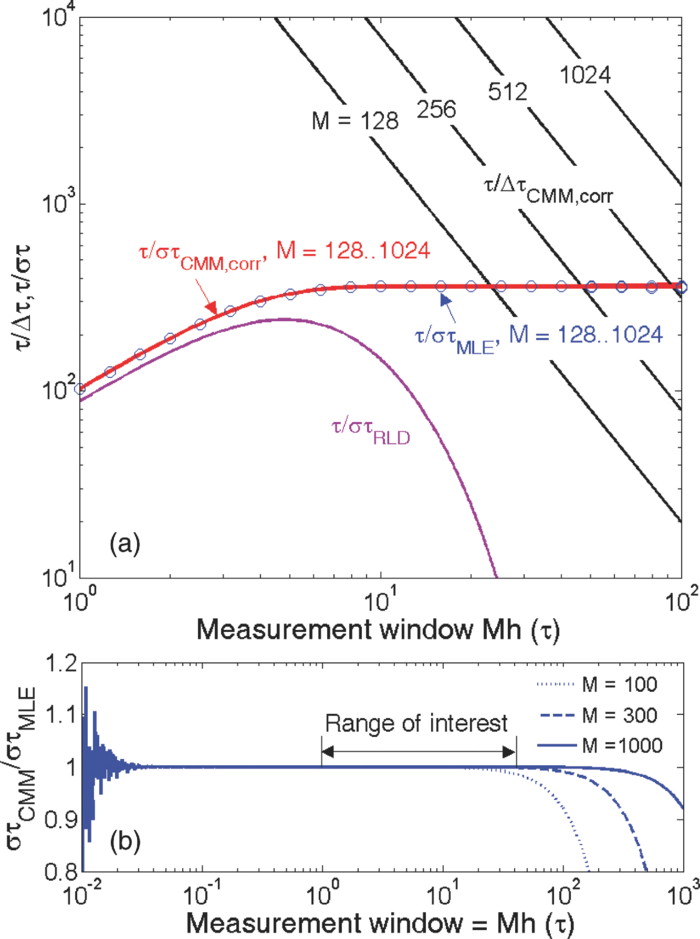
1.IntroductionA single-photon avalanche diode (SPAD), when biased at above its breakdown voltage, can be triggered by a photon that results in a self-sustaining avalanche multiplication process.1 Its gain is so large that its output current can be easily converted into a digital signal without using complex front-end amplifiers deteriorating the signal-to-noise (SNR) ratio.2 With such single-photon sensitivity, SPADs are suitable for photon-starved applications such as single molecule detection.3, 4 Thanks to the progress of semiconductor technology, SPAD arrays have been fabricated in a low-cost complementary metal-oxide-semiconductor (CMOS) process for three dimensional ranging and fluorescence lifetime sensing applications.5, 6, 7, 8 The doubt about higher dark count caused by exacerbated tunneling effect on an advanced CMOS process has been dispelled by the latest developments in deep sub-micron SPAD structures.9, 10, 11, 12 A dark count rate (DCR) of 25 Hz has been successfully reported in standard 0.13 μm CMOS process,10 and low dark-count prototypes moving to 90 nm CMOS process node to miniaturize the pixel size or to enhance the quantum efficiency in the near-infrared spectral range have also been recently published.11, 12 Much larger SPAD arrays can be expected to facilitate fluorescence lifetime imaging microscopy (FLIM) applications. Packing SPADs in arrays provides more flexibility as SPADs can work independently or in a group in combination with a multi-beam confocal imaging microscope.13 The SPAD array can provide a platform for both wide-field and confocal scanning microscopy. In the past, fluorescence lifetime imaging with high spatial resolution has been achieved by applying confocal scanning microscopes. The fluorescence histogram was recorded by a high-resolution time-to-digital converter (TDC) in a time-correlated single-photon counting (TCSPC) module. The data was stored in memory and then post-processed using maximum-likelihood-estimation (MLE) or least-square method (LSM)-based curve-fitting software pixel-by-pixel to generate a lifetime image. Although the MLE (or LSM) has merits of wide resolvability range and high photon efficiency, and usually hundreds of photons are enough to reach an acceptable accuracy,14, 15 the data acquisition is still slow (measurement time = N x × N y/f p, where f p is the scanning frequency and N x × N y is the dimension of the array) and limits the systems to imaging only stationary objects. In many biological applications, real-time FLIM imaging for monitoring cell dynamics in low light level is desirable. There are real-time time-domain and frequency-domain FLIM systems available for wide-field applications. The time-domain FLIM systems usually employ time-gated detection.16 Gated intensified charge-coupled device (CCD) cameras with a tunable delay from the excitation pulse and a given gate width are typically used to construct the fluorescence decay. Usually, a series of intensity images at different delays are acquired to generate a lifetime image, and attempts to solve double-exponential decays with multiple gates have also been reported.17 For wide-field frequency domain FLIMs, they are typically implemented using optical image intensifiers.18, 19 Directly modulating the gain of a CCD camera has also been implemented.20 Most of the systems mentioned above are CCD-based with multiple-channel plate intensifiers and usually require high voltage supplies (tens to hundreds of volts) or cooling systems. The quantum efficiency, DCR, physical size, spectral detection range, and required driving voltage for the latest reported SPADs, on the other hand, have been greatly improved during the past two years 6, 7, 8, 9, 10, 11, 12 This enables rapid advances in the development of high-speed FLIM cameras. With such SPAD-based systems we aim to provide: 1. fast lifetime previews, 2. intensity/lifetime imaging, 3. raw arrival time for detailed analysis, 4. a platform for both wide-field and confocal scanning microscopy, 5. compact, low voltage, and low cost solutions, and 6. flexibility to configure the cameras for other applications, such as fluorescence correlation spectroscopy (FCS) or Förster resonance energy transfer. We have proposed a high-speed digital FLIM algorithm for a lifetime sensing system based on the center of mass method (CMM), and demonstrated its feasibility on real data collected by a single 0.35 μm CMOS SPAD and a single photon multiplier tube system.14 It was proven to be suitable for sensing and confocal scanning applications. To apply the CMM for imaging applications, we need to collect arrival time information of every detected photon event for each pixel. This can be achieved by integrating TDCs in-pixel. Richardson reported a low power 10-bit TDC array (with fast and slow TDC test sub-arrays)21 with integrated low dark count SPADs (Ref. 10) to create a single chip TCSPC sensor in a 0.13 μm standard CMOS imaging process. The chip operates at a frame rate of 1 MHz and contains global calibration circuitry to maintain uniformity, and a time resolution of 54 ps has been achieved. The quantum efficiency of the SPAD is 28% at a wavelength of 500 nm with 80% of the pixels below a DCR of 50 Hz at room temperature. The imager can operate in a time-correlated mode for lifetime imaging or in a time-uncorrelated mode for intensity imaging. It can also be configured for confocal scanning and FCS applications13 such that multiple SPAD pixels can be grouped together and greatly improve the photon collecting speed. The in-pixel TDCs can generate raw arrival time data, which can be sent to a PC and post-processed by curve fitting software. To increase the imaging speed, the raw arrival time data can be processed by on-field programmable gate array (FPGA) CMM processors. With CMM, video-rate FLIM imaging for biological applications can be achieved. Figures 1a, 1b, 1c show the imager assembly including a 32×32 SPAD plus TDC chip and an Opal Kelly board containing a Xilinx Spartan-III FPGA,22 on which the CMM is implemented. Fig. 1(a) Top view, (b) bottom view of imager assembly with a 32×32 CMOS SPAD + TDC chip and an Opal Kelly board containing a Xilinx Spartan-III FPGA, and (c) 32×16 SPAD + TDC array and FPGA implementation of CMM.  The full range of TDCs should be able to accommodate commonly used samples with fluorescence lifetime, ranging from sub-nanosecond to tens of nanoseconds. Applying previously proposed CMM (Ref. 14) on a 10-bit TDC array with 54 or 78 ps resolution (TDC full range = 55 or 80 ns) will limit the lifetime resolvability range to less than 8 or 11 ns (τ < T/7). To alleviate this problem, we can either apply TDCs with tunable resolution or simply employ a look-up table on-FPGA or with software without adding extra cost. The motivation of our paper is to develop low-cost hardware algorithms that can not only generate fast previews of the lifetime data but also remove I/O bottlenecks by compressing the raw timing data. For simplicity and for a low cost solution, we assume the fluorescence emission is a single-exponential decay. The single-exponential decay model, however, is still useful to contrast different types of fluorophores. For diagnostic applications, obtaining lifetime contrast is probably more important than calculating the absolute values of lifetimes.16 End-users can use the proposed algorithms to generate high-speed wide-field previews of lifetime data and switch to record raw data in wide-field or confocal scanning systems to produce high-resolution imaging on the area-of-interest. High-speed preview images are particularly useful for recording flow or protein-protein dynamics in live cells with minimum hardware/software resources. In this paper, we first introduce a simple lifetime correction method that can be either implemented on firmware or software to enhance the lifetime resolvability range of the proposed CMM algorithm. The error equations for the corrected CMM algorithm will be given in Sec. 2. The correction allows the application of a higher laser repetition rate and therefore decreases the acquisition time. The FPGA implementation for the proposed algorithm on a low noise 32×32 0.13 μm CMOS SPAD plus TDC array will be introduced in Sec. 2. Image analysis of the SPAD array and video-rate FLIM will be presented in Sec. 3. 2.Material and Methods2.1.Fluorescence Lifetime Imaging Microscopy Algorithm Using Center-of-Mass MethodFor a fluorescence histogram with a single-exponential decay f(t) = Aexp(−t/τ) in a measurement window 0 ⩽ t ⩽ Trecorded by the in-pixel 10-bit TDC,21 its center of mass (CM) is approximated to the lifetime τ Eq. 1[TeX:] \documentclass[12pt]{minimal}\begin{document}\begin{eqnarray} {\rm CM} &=& \frac{{\int_0^T {tf(t)} dt}}{{\int_0^T {f(t)} dt}} = \tau - \frac{{T{\mathop{\rm e}\nolimits} ^{ - T/\tau } }}{{1 - {\mathop{\rm e}\nolimits} ^{ - T/\tau } }}\nonumber\\ & \cong & \tau _{{\rm CMM}} = \left({\frac{{\displaystyle\sum\limits_{j = 0}^{M - 1} {jN_j } }}{{N_c }} + \frac{1}{2}} \right)h, \end{eqnarray}\end{document}Eq. 2[TeX:] \documentclass[12pt]{minimal}\begin{document}\begin{equation} \frac{{\Delta \tau _{CMM} }}{\tau } = \frac{h}{\tau }G(x) - 1, \end{equation}\end{document}Eq. 3[TeX:] \documentclass[12pt]{minimal}\begin{document}\begin{equation} \frac{{\sigma \tau _{CMM} }}{\tau } = \frac{h}{{\tau \sqrt {N_c } }}\frac{{\sqrt {P(x)} }}{{({1 - x})({1 - x^M })}}, \end{equation}\end{document}Eq. 4[TeX:] \documentclass[12pt]{minimal}\begin{document}\begin{equation} G(x) = \frac{{1 + x}}{{2({1 - x})}} - \frac{{Mx^M }}{{1 - x^M }}, \end{equation}\end{document}Eq. 5[TeX:] \documentclass[12pt]{minimal}\begin{document}\begin{equation} P(x) = x - M^2 x^M + ({2M^2 - 2})x^{M + 1} - M^2 x^{M + 2} + x^{2M + 1}, \end{equation}\end{document}2.2.Enhancing Resolvability Range of Center of Mass MethodThe calculated lifetime τ CMM only approximates to the exact one τ as a measurement window T > 7τ. For T < 7τ, Eq. 1 becomes a biased estimator, and it quickly converges to a less uncertain but wrong estimation smaller than the actual lifetime. To enhance the lifetime resolvability range, Eq. 1 needs to be re-examined. When T < 7τ is employed, the term Texp(–T/τ)/[1 – exp(–T/τ)] in Eq. 1 cannot be neglected, and Eq. 1 is rewritten as Eq. 6[TeX:] \documentclass[12pt]{minimal}\begin{document}\begin{equation} \frac{{\tau _{{\rm CMM}} }}{T} = \frac{\tau }{T} - \frac{{{\mathop{\rm e}\nolimits} ^{ - T/\tau } }}{{1 - {\mathop{\rm e}\nolimits} ^{ - T/\tau } }}. \end{equation}\end{document}Eq. 7[TeX:] \documentclass[12pt]{minimal}\begin{document}\begin{equation} \frac{{\tau _{i + 1} }}{T} = \frac{{\tau _{{\rm CMM}} }}{T} + \frac{{{\mathop{\rm e}\nolimits} ^{ - T/\tau _i } }}{{1 - {\mathop{\rm e}\nolimits} ^{ - T/\tau _i } }}, \end{equation}\end{document}Eq. 8[TeX:] \documentclass[12pt]{minimal}\begin{document}\begin{eqnarray} \frac{{\Delta \tau _{CMM,Corr} }}{\tau } &=& \frac{h}{\tau }G(x) - 1 + \frac{{T{\mathop{\rm e}\nolimits} ^{ - T/\tau } }}{{\tau ({1 - {\mathop{\rm e}\nolimits} ^{ - T/\tau } })}}\nonumber\\ & = & \frac{h}{\tau }G(x) - 1 \!+\! \frac{h}{\tau }\frac{{M{\mathop{\rm e}\nolimits} ^{ - Mh/\tau } }}{{1 - {\mathop{\rm e}\nolimits} ^{ - Mh/\tau } }} = \frac{h}{\tau }\frac{{1 + x}}{{2({1 - x})}} \!-\! 1,\nonumber\\ \end{eqnarray}\end{document}Eq. 9[TeX:] \documentclass[12pt]{minimal}\begin{document}\begin{eqnarray} \frac{{\sigma \tau _{CMM,Corr} }}{\tau } &=& \frac{{\sigma \tau _{CMM} }}{\tau } \left({\frac{{d\tau _{CMM} }}{{d\tau }}} \right)\nonumber\\ & = & \frac{h}{{\tau \sqrt {N_c } }}\frac{{\sqrt {P(x)} ({1 - x^M })}}{{({1 {-} x})\big[ {({1 {-} x^M })^2 {-} \frac{{M^2 h^2 }}{{\tau ^2 }}x^M }\big]}}{\rm.} \end{eqnarray}\end{document}Eq. 10[TeX:] \documentclass[12pt]{minimal}\begin{document}\begin{equation} \frac{{\sigma \tau _{MLE} }}{\tau } = \frac{\tau }{{h\sqrt {N_c } }}\frac{{({1 - x})({1 - x^M })}}{{\sqrt {P(x)} }}{\rm.} \end{equation}\end{document}2.3.On-FPGA Implementation of Center of Mass Method for Low Dark Count Single-photon Avalanche Diode ArraysWe rewrite Eq. 1 as Eq. 11[TeX:] \documentclass[12pt]{minimal}\begin{document}\begin{equation} \frac{{\tau _{CMM} }}{h} = \frac{{\sum\limits_{i = 1}^{N_c } {\bar D_i } }}{{N_c }} + \frac{1}{2}, \end{equation}\end{document}Eq. 12[TeX:] \documentclass[12pt]{minimal}\begin{document}\begin{equation} N_c = 2^L,L\,{\rm is\, an\, integer}, \end{equation}\end{document}Eq. 13[TeX:] \documentclass[12pt]{minimal}\begin{document}\begin{equation} \tau = \Omega \left({\frac{{\tau _{CMM} }}{T}} \right) \cdot T = \Omega \left[ {\frac{1}{M}\left({\frac{{\displaystyle\sum\limits_{i = 1}^{N_c } {\bar D_i } }}{{N_c }} + \frac{1}{2}} \right)} \right] \cdot Mh, \end{equation}\end{document}3.Experimental Results3.1.Corrected CMM Fluorescence Lifetime Imaging Analysis on DNA MicroarraysTo evaluate the suitability of CMM for fluorescence lifetime imaging applications in realistic experimental conditions we first present post-processed (software-based) CMM of TCSPC data collected from DNA microarrays.27 DNA microarrays consisting of 16 spots where incubated with (a) hepatitis C virus (HCV) probe, (b) human cytomegalovirus (HCMV) probe, and (c) a 1:1 molar ratio of these two probes. The arrays were hybridized with a 10-nM solution of fluorescently labeled complementary targets with a distinctly different excited state lifetime: HCV targets were labeled with Alexa Fluor 430 and HCMV with quantum dot (Qdot525) with lifetimes of approximately 4.2 and 22 ns,28 respectively. The labeled microspot arrays were imaged using total internal reflection fluorescence (TIRF) illumination and TCSPC histograms were recorded using 32×16 SPAD + TDC array with 55 ns range. Details of the experimental procedures are given elsewhere.27 Figure 4a shows a fluorescence histogram collected by a pixel, a tail-fitted decay using the proposed CMM, and the residual plot for the Qdot525 labeled HCMV probes. Figure 4b shows the estimated lifetime and precision curves versus the measurement window (M = 200 to 800; 0.5 < T/τ < 2) for different algorithms. The uncorrected CMM, Eq. 1, suffers a significant bias even with the maximum measurement window the TDC can provide. For M = 200, the uncorrected CMM obtains a lifetime of 5 ns, which is far from the reality! The results obtained by the corrected CMM, Eqs. 7 or 13 converge to those obtained by the MLE as M increases and are slightly better than those by RLD, which is in good agreement with Fig. 2a. The corrected CMM can extend the resolvability range down to Mh = 0.5τ, but the measurement window is usually chosen as Mh = 2 to 5τ for better precision. Figure 4c shows the photon count (intensity) and lifetime images for the 10 nM Qdot525 labeled microspots using M = 500. Fig. 4(a) Fluorescence histogram and residual curves obtained by the proposed CMM, (b) lifetime and precision curves for different algorithms, and (c) intensity and lifetime images of quantum-dot labeled DNA microarray using M = 500. 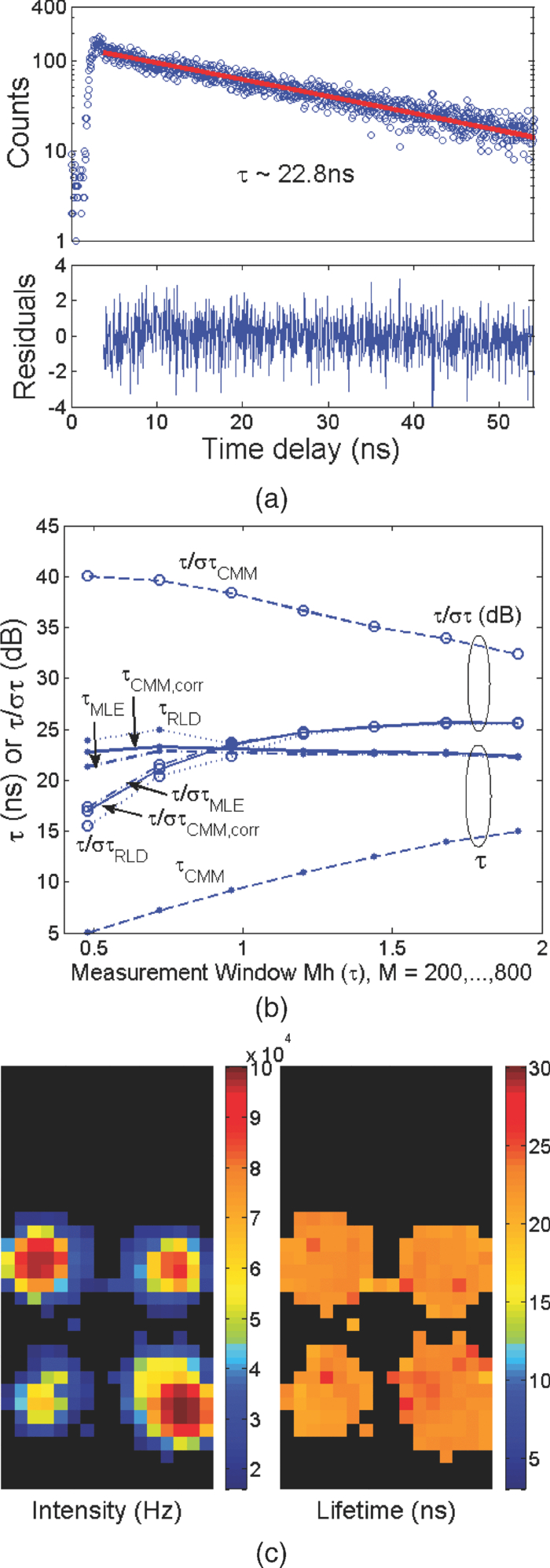 The analysis can be repeated for Alexa labeled HCV microspots. Figure 5a shows a fluorescence histogram collected by a pixel, a tail-fitted decay using the proposed CMM, and the residual plot. Figure 5b shows the estimated lifetime and precision versus the measurement window (M = 100 to 800; 1 < T/τ < 10) for different algorithms. As the signal levels are lower, the background plays a more significant role and contributes to the loss of precision for a larger M. There exists a trade-off between samples with different lifetimes. Nevertheless, the algorithm provides reliable lifetime estimates when simultaneously imaging differently labeled spots as shown in Fig. 6a using M = 500. The lifetime map and the corresponding lifetime histogram shown in Fig. 6b are in good agreement with the results reported in Ref. 27, Fig. 3d. Note that for the two mixed (both labels present) spots the delay is clearly multi-exponential. CMM returns an estimate of the average lifetime, losing information about the decay dynamics but providing enough contrast to clearly distinguish the three types of microspots. From Eq. 1, for a double-exponential decay f(t) = A 1exp(−t/τ 1) + A 2exp(−t/τ 2), the calculated lifetime using the uncorrected CMM is Eq. 14[TeX:] \documentclass[12pt]{minimal}\begin{document}\begin{eqnarray} && \hspace{-.6pc}\tau _{{\rm CMM}}\nonumber\\ && \cong \frac{{\int_0^T {tf(t)} dt}}{{\int_0^T {f(t)} dt}}\nonumber\\ && = \frac{ {A_1 \tau _1^2 {\mathop{\rm e}\nolimits} ^{ - t/\tau _1 } \left({ - \frac{t}{{\tau _1 }} - 1} \right)} \Big|_0^T + {A_2 \tau _2^2 {\mathop{\rm e}\nolimits} ^{ - t/\tau _2 } \left({ - \frac{t}{{\tau _2 }} - 1} \right)} \Big|_0^T }{{ { - A_1 \tau _1 {\mathop{\rm e}\nolimits} ^{ - t/\tau _1 } } |_0^T { - A_2 \tau _2 {\mathop{\rm e}\nolimits} ^{ - t/\tau _2 } } |_0^T }}. \nonumber\\ &&= \frac{{A_1 \tau _1^2 \!-\! A_1 \tau _1^2 {\mathop{\rm e}\nolimits} ^{ - T/\tau _1 } \left({\frac{T}{{\tau _1 }} \!+\! 1} \right) \!+\! A_2 \tau _2^2 \!-\! A_2 \tau _2^2 {\mathop{\rm e}\nolimits} ^{ - T/\tau _2 } \left({\frac{T}{{\tau _2 }} \!+\! 1} \right)}}{{A_1 \tau _1 - A_1 \tau _1 {\mathop{\rm e}\nolimits} ^{ - T/\tau _1 } \!+\! A_2 \tau _2 - A_2 \tau _2 {\mathop{\rm e}\nolimits} ^{ - T/\tau _2 } }},\!\!\! \nonumber\\ \end{eqnarray}\end{document}3.2.Fluorescence Lifetime Estimation Based on Low Number of Photon Events3.2.1.Fluorescence lifetime imaging on Rhodamine BTo achieve high-speed FLIM imaging, it is desirable to study the error performance when using a low number of photon events. For experimental demonstration of the CMM hardware lifetime calculation algorithm, a standard fluorescence lifetime wide-field imaging system was set up on a Nikon TE2000U inverted microscope. The excitation source was a PicoQuant pulsed diode laser with a wavelength of 470 nm coupled through the epi-fluorescence port of the microscope using a Nikon B-2A filter cube. The laser pulse rate is 20 MHz and the maximum power reaching the back focal plane of the objective is about 90 μW. The sample was imaged onto the 32×32 SPAD camera directly attached to one of the camera ports using a 20× objective (Nikon Plan Apo, 20×, NA 0.45). The TDC resolution is set to be 78 ps with the on-chip phase-locked loop enabled.21 The IRF was measured by replacing the sample with a mirror and removing the emission filter so that the excitation light was found to have a FWHM of 0.6 ns. First, a uniform sample of an aqueous solution of Rhodamine B was imaged, which makes it possible to assess the influence of inter-pixel variations. Each pixel has its own physically distinct SPAD and TDC leading to slightly different characteristics for each pixel. About 13% of the SPADs have a DCR in excess of 500 Hz and the peak position of the IRF has a standard deviation of about five bins due to variations in the time offset. We used the raw data stored in the memory to predict the error performance of the on-FPGA CMM. A measurement window of 100h (M = 100; Mh/τ ∼ 4.1) was chosen to calculate lifetimes. Two global window parameters FIRST and LAST (= FIRST + M − 1) can be set by users even without knowing the precise peak position of each IRF. For more accurate imaging, IRFs of all the pixels can be recorded, and the shift of their peak positions ΔFIRST relative to FIRST, can be added to the detected TDC value for each pixel such that the peaks for all histograms would align for the best photon efficiency. For fast demonstration, we only implemented the blue blocks of Fig. 3 on FPGA with a global FIRST set to all pixels (denoted as the global scheme hereafter). Figure 7a shows lifetime images obtained by the corrected CMM, for an average N c = 335, 677, 1376, and 2774, respectively, with FIRST set for each pixel to the peak of its own histogram (denoted as the local scheme hereafter), but without the noisy pixels [∼13% of pixels with DCR > 500 Hz (Ref. 21)] removed. The pattern of noisy pixels can be easily spotted, and it can be located during the characterization of the imager. It is desirable to exclude these noisy pixels to solely reveal the error performance of the algorithms. We applied simple median filtering only on the noisy pixels, and the lifetime images are shown as Fig. 7b. Figure 7c shows lifetime images for an average N c = 281, 562, 1123, and 2244, respectively, using the global scheme, which will be similar to the images generated from the on-FPGA CMM. Figure 7d shows lifetime versus N c scattergrams with the noisy pixels excluded. From Eq. 9, the precision for the corrected CMM is about 3log2(N c) – 1.5 (dB) at Mh/τ ∼ 4.1 [ [TeX:] $F \equiv \sqrt {N_c } \cdot {{\sigma \tau } / \tau } = 1.2$ (Ref. 29)]. Figures 7e and 7f show the precision curves versus N c with the local and global schemes, respectively. The measurement window for RLD was chosen at its optimum condition for a fair comparison. The global scheme contributes to 1 to 2 dB of loss in precision and a bias of 0.03 ns due to some pixels having their peaks away from FIRST, but we can expect the loss will be smaller for resolving samples with larger lifetimes. The error performance of the corrected CMM is similar to that of MLE. With the global scheme, the proposed CMM can extract lifetimes with an SNR of 22 dB with only 281 counts (F ∼ 1.3). The ideal curve is based on the MLE,15 but without considering nonidealities of the system, such as jitter, uniformity, etc. The deviation from the ideal curve (note the F value is not 1.0, since we use a measurement window of 4.1τ where the optimum F = 1.2) comes from nonidealities such as jitter of the IRF, nonuniformity of the TDC resolution, and background, etc. Nevertheless, it provides reliable lifetime estimates and is enough for high-speed FLIM. Fig. 7(a) and (b) Lifetime images for different N c with local FIRST scheme without and with noisy pixels filtered respectively, (c) lifetime images for different N c with a global FIRST, (d) lifetime versus photon count scattergrams with noisy pixels excluded, precision plots with (e) the local scheme and (f) a global FIRST.  3.2.2.Fluorescence lifetime imaging on fluorescent beads in Rhodamine 6GIn order to study the error performance of the proposed on-FPGA CMM, we prepared a simple sample showing two distinct but similar lifetimes by suspending yellow-green fluorescent polystyrene beads of 15 μm diameter (Invitrogen, FluoSpheres, F8844) in an aqueous solution of Rhodamine 6G. The fluorescent solution was prepared very concentrated (1 mM) in order to achieve signal levels comparable to the bright beads. But, before we demonstrate video-rate FLIM imaging on fluorescent beads in Rhodamine 6G, it is desirable to study the error performance of the proposed on-FPGA CMM on a static sample. By doing so, we can expect what we are going to see on the video. We choose M = 250 (Mh ∼ 5τ for Rhodamine 6G and Mh ∼ 4τ for the beads) and a global FIRST for the whole array. Figure 8a shows the lifetime images of a fluorescent bead in Rhodamine 6G for an average N c of 430, 862, 1726, and 3454, respectively. Figure 8b shows the scattergram of the lifetimes versus the photon counts for the RLD (gate width w g = 2 ∼ 2.5τ) and corrected CMM. The measurement window for RLD was chosen at its optimum condition for a fair comparison. Figures 8c and 8d show the precision plots for Rhodamine 6G and beads, respectively. The error performance of the corrected CMM is similar to that of MLE. The CMM performs better than RLD for resolving Rhodamine 6G with a margin of 2 dB. The number of pixels covering the bead is small, and that is why we have a higher deviation. The lifetimes can be estimated from the lifetime histograms and they are 3.8 ns for Rhodamine 6G and 5.0 ns for the bead, both in good agreement with the data provided by the manufacturers. 3.3.Video-Rate Fluorescence Lifetime Imaging on Fluorescent Beads in Rhodamine 6GTo demonstrate video-rate performance, the sample stage holding a sample of fluorescent beads in Rhodamine 6G was translated, simulating flow of tracer particles in a microfluidic cell sorter system. From the discussion in Sec. 3.2, we choose M = 250, a global FIRST for the whole array, and L = 10 (N c = 1024). Figure 9a (1) shows the first frame of the lifetime image and the corresponding lifetime histogram of the video, 240 frames in total. The lifetime images are generated at a frame speed of 50 fps (lifetimes updated at a rate higher than 100 Hz), but the video is played at a ×0.6 speed, 30 fps. We applied median filtering to remove the noisy pixels on FLIM images, and the noisy pixels were also excluded from the lifetime histogram solely to reveal the performance of the proposed algorithm. Figure 9b shows the 72nd to 76th frames of lifetime images and their corresponding lifetime histograms, respectively, as a new bead goes into the field of view. The size of the bead is 15 μm. The speed of the translating stage reaches up to 200 μm/s. The 76th frame contains two beads, and the lifetimes of the Rhodamine 6G and the beads with noisy pixels removed are 3.8 ns (στ ∼ 0.19 ns) and 5.0 ns (στ ∼ 0.25 ns), respectively. Their precisions are both around 26 dB close to the estimation on the precision plots shown in Figs. 8c and 8d. Figures 9c and 9d show the estimated lifetimes of the pixels (14, 12) marked as “O” and (6, 16) marked as “P” versus the frame number, respectively. During the video recording, the sample stage was initially static for 15 frames and it started to move. The top speed can be observed from the 72nd to 76th frames. After that, it was slowed down and then moved backward from the 160th frame. Throughout the video, only one bead passed the pixel (14, 12), whereas two beads passed the pixel (6, 16) with the first bead marginally passing it once and the second one passing it forward and backward with different speeds. Fig. 9(a) (1) Fluorescence lifetime movie of fluorescent beads (τ = 5 ns) in Rhodamine 6G (τ = 3.8 ns), (b) 72nd to 76th frames of lifetime images and their corresponding lifetime histograms, respectively, and (c) and (d) estimated lifetimes of the pixels O (14, 12) and P (6, 16) versus the frame number, respectively. (1, Quicktime, 5.7 MB)  4.ConclusionA newly proposed FPGA algorithm for single-detector fluorescence lifetime sensing systems, CMM, has been successfully improved and employed for high-speed FLIM imaging applications. It can be viewed as a hardware implementation algorithm for the commonly used MLE method, as it has very similar performance but only needs a simple 1D LUT rather than a 2D LUT that depends on both M and h. To demonstrate its performance, a wide-field microscope was adapted to accommodate a 0.13 μm CMOS 32×32 SPAD + TDC array to test different fluorescent samples. Video-rate FLIM imaging with a frame rate over 50 fps can be achieved and has been demonstrated on fluorescent beads in Rhodamine 6G. The calculated lifetimes are in good agreement with those obtained by commercially available software. To enhance the lifetime resolving range, the previously proposed algorithm has been modified by introducing a LUT on software and demonstrated on real data. We can expect our FLIM camera prototype with future improvements on firmware/software and with the mounted micro-lens array to improve sensitivity30 to provide new applications for cellular imaging, such as proteomics, DNA microarray scanning, flow engineering, protein-DNA interactions,31 and tissue imaging.32 AcknowledgmentsThe CMM hardware implementation and data analysis have been supported by the European Commission within the 7th Framework Programme, Health Research METOXIA project (HEALTH-F2–2009-222741, www.metoxia.uio.no). Tyndall is sponsored by an EPSRC Studentship. The CMOS SPAD chip has been supported by the European Commission within the 6th Framework Programme of the Information Science Technologies, Future Emerging Technologies Open MEGAFRAME project (Contract No. 029217–2, www.megaframe.eu). The authors would like to thank Dr. Wei Wang for his comments on this work. ReferencesS. Cova, M. Ghioni, A. Lacaita, C. Samori, and
F. Zappa,
“Avalanche photodiodes and quenching circuits for single-photon detection,”
Appl. Opt., 35 1956
–1976
(1996). https://doi.org/10.1364/AO.35.001956 Google Scholar
S. Cova, M. Ghioni, A. Lotito, I. Rech, and
F. Zappa,
“Evolution and prospects for single-photon avalanche diodes and quenching circuits,”
J. Mod. Opt., 51 1267
–1288
(2004). Google Scholar
L.-Q. Li and
L. M. Davis,
“Single photon avalanche diode for single molecule detection,”
Rev. Sci. Instrum., 64 1524
–1529
(1993). https://doi.org/10.1063/1.1144463 Google Scholar
H. Yang, G. Luo, P. Karnchanaphanurach, T.-M. Louie, I. Rech, S. Cova, L. Xun, and
X. S. Xie,
“Protein conformational dynamics probed by single-molecule electron transfer,”
Science, 10 262
–266
(2003). https://doi.org/10.1126/science.1086911 Google Scholar
C. Niclass, A. Rochas, P. A. Besse, and
E. Charbon,
“Design and characterization of a CMOS 3-D image sensor based on single photon avalanche diodes,”
IEEE J. Solid-State Circuits, 40 1847
–1853
(2005). https://doi.org/10.1109/JSSC.2005.848173 Google Scholar
D. Stoppa, D. Mosconi, L. Pancheri, and
L. Gonzo,
“Single-photon avalanche diode CMOS sensor for time-resolved fluorescence measurements,”
IEEE Sens. J., 9 1084
–1090
(2009). https://doi.org/10.1109/JSEN.2009.2025581 Google Scholar
D. E. Schwartz, P. Gong, and
K. L. Shepard,
“Time-resolved Förster-resonance-energy-transfer DNA assay on an active CMOS microarray,”
Biosens. Bioelectron., 24 383
–390
(2008). https://doi.org/10.1016/j.bios.2008.04.015 Google Scholar
B. R. Bae, K. J.-B. Yang, J. McKendry, Z. Gong, D. Renshaw, J. M. Girkin, E. Gu, M. D. Dawson, and
R. K. Henderson,
“A vertically integrated CMOS microsystem for time-resolved fluorescence analysis,”
IEEE Trans. Biomed. Circ. Syst., 4 437
–444
(2010). https://doi.org/10.1109/TBCAS.2010.2077290 Google Scholar
M. Gersbach, J. Richardson, E. Mazaleyrat, S. Hardillier, C. Niclass, R. Henderson, L. Grant, and
E. Charbon,
“A low-noise single-photon detector implemented in a 130 nm CMOS imaging process,”
Solid-State Electron., 53 803
–808
(2009). https://doi.org/10.1016/j.sse.2009.02.014 Google Scholar
J. A. Richardson, L. A. Grant, and
R. K. Henderson,
“Low dark count single-photon avalanche diode structure compatible with standard nanometer scale CMOS technology,”
IEEE Photon. Technol. Lett., 21 1020
–1022
(2009). https://doi.org/10.1109/LPT.2009.2022059 Google Scholar
R. K. Henderson, E. A. G. Webster, R. Walker, J. A. Richardson, and
L. A. Grant,
“A 3×3, 5 mm pitch, 3-transistor single photon avalanche diode array with integrated 11 V bias generation in 90 nm CMOS technology,”
14.2
(2010). Google Scholar
E. A. G. Webster, J. A. Richardson, L. A. Grant, D. Renshaw, and
R. K. Henderson,
“An infra-red sensitive, low noise, single-photon avalanche diode in 90 nm CMOS,”
International Image Sensor Workshop (IISW), 8
–11 Hokkaido, Japan
(June 2011). Google Scholar
R. A. Colyer, G. Scalia, I. Rech, A. Gulinatti, M. Ghioni, S. Cove, S. Weiss, and
X. Michalet,
“High-throughput FCS using an LCOS spatial light modulator and an 8×1 SPAD array,”
Biomed. Opt. Express, 1 1408
–1430
(2010). https://doi.org/10.1364/BOE.1.001408 Google Scholar
D.-U. Li, B. Rae, R. Andrews, J. Arlt, and
R. Henderson,
“Hardware implementation algorithm and error analysis of high-speed fluorescence lifetime sensing systems using center-of-mass method,”
J. Biomed. Opt., 15 017006
(2010). https://doi.org/10.1117/1.3309737 Google Scholar
P. Hall and
B. Selinger,
“Better estimates of exponential decay parameters,”
J. Phys. Chem., 85 2941
–2946
(1981). https://doi.org/10.1021/j150620a019 Google Scholar
D. S. Elson, I. Munro, J. Requejo-Isidro, J. McGinty, C. Dunsby, N. Galletly, G. W. Stamp, M. A. A. Neil, M. J. Lever, P. A. Kellett, A. Dymoke-Bradshaw, J. Hares, and
P. M. W. French,
“Real-time time-domain fluorescence lifetime imaging including single-shot acquisition with a segmented optical image intensifier,”
New J. Phys., 6 1
–13
(2004). https://doi.org/10.1088/1367-2630/6/1/180 Google Scholar
M. Elangovan, R. N. Day, and
A. Periasamy,
“Nanosecond fluorescence resonance energy transfer-fluorescence lifetime imaging microscopy to localize the protein interactions in a single living cell,”
J. Microsc., 205 3
–14
(2002). https://doi.org/10.1046/j.0022-2720.2001.00984.x Google Scholar
G. I. Redford and
R. M. Clegg,
“Real-time fluorescence lifetime imaging and FRET using fast gated intensifiers,”
Molecular Imaging: FRET Microscopy and Spectroscopy, 193
–226 Oxford University, New York
(2005). Google Scholar
A. Leray, F. B. Riquet, E. Richard, C. Spriet, D. Trinel, and
L. Héliot,
“Optimized protocol of a frequency domain fluorescence lifetime imaging microscope for FRET measurements,”
Microsc. Res. Tech., 72 371
–379
(2009). https://doi.org/10.1002/jemt.20665 Google Scholar
A. C. Mitchell, J. E. Wall, J. G. Murray, and
C. G. Morgan,
“Direct modulation of the effective sensitivity of a CCD detector: a new approach to time-resolved fluorescence imaging,”
J. Microsc., 206 225
–232
(2002). https://doi.org/10.1046/j.1365-2818.2002.01029.x Google Scholar
J. Richardson, R. Walker, L. Grant, D. Stoppa, F. Borghetti, E. Charbon, M. Gersbach, and
R. Henderson,
“A 32×32 50 ps resolution 10 bit time to digital converter array in 130 nm CMOS for time correlated imaging,”
Proc. IEEE Custom Integrated Circuits Conf. (CICC), 77
–80 San Jose, CA
(2009). Google Scholar
, Datasheet DS099 (v2.5), Xilinx, Inc., San Jose, CA (
(2009) Google Scholar
R. M. Ballew and
J. N. Demas,
“An error analysis of the rapid lifetime determination method for the evaluation of single exponential decays,”
Anal. Chem., 61 30
–33
(1989). https://doi.org/10.1021/ac00176a007 Google Scholar
A. V. Agronskaia, L. Tertoolen, and
H. C. Gerritsen,
“Fast fluorescence lifetime imaging of calcium in living cells,”
J. Biomed. Opt., 9 1230
–1237
(2004). https://doi.org/10.1117/1.1806472 Google Scholar
D.-U. Li, B. Rae, E. Bonnist, D. Renshaw, and
R. Henderson,
“On-chip fluorescence lifetime extraction using synchronous gating scheme: theoretical error analysis and practical implementation,”
Proc. Int. Conf. Bio-inspired Systems and Signal processing, 171
–176 Funchal, Portugal
(2008). Google Scholar
C. Moore, S. P. Chan, J. N. Demas, and
B. A. Degraff,
“Comparison of methods for rapid evaluation of lifetime of exponential decays,”
Appl. Spectrosc., 58 603
–607
(2004). https://doi.org/10.1366/000370204774103444 Google Scholar
G. Giraud, H. Schulze, D.-U. Li, T. T. Bachmann, J. Crain, D. Tyndall, J. Richardson, R. Walker, D. Stoppa, E. Charbon, R. Henderson, and
J. Arlt,
“Fluorescence lifetime biosensing with DNA microarrays and a CMOS-SPAD imager,”
Biomed. Opt. Express, 1 1302
–1308
(2010). https://doi.org/10.1364/BOE.1.001302 Google Scholar
G. Giraud, H. Schulze, T. T. Bachmann, C. J. Campbell, A. R. Mount, P. Ghazal, M. R. Khondoker, A. J. Ross, S. W. J. Ember, I. Ciani, C. Tlili, A. J. Walton, J. G. Terry, and
J. Crain,
“Fluorescence lifetime imaging of quantum dot labeled DNA microarrays,”
Int. J. Mol. Sci., 10 1930
–1941
(2009). https://doi.org/10.3390/ijms10041930 Google Scholar
A. Draaijer, R. Sanders, and
H. C. Gerritsen,
“Fluorescence lifetime imaging, a new tool in confocal microscopy,”
Handbook of Biological Confocal Microscopy, 491
–505 Plenum, New York
(1995). Google Scholar
S. Donati, G. Martini, and
M. Norgia,
“Microconcentrators to recover fill-factor in image photodetectors with pixel on-board processing circuits,”
Opt. Express, 15 18066
–18075
(2007). https://doi.org/10.1364/OE.15.018066 Google Scholar
F. G. E. Cremazy, E. M. M. Manders, P. I. H. Bastiaens, G. Kramer, G. L. Hager, E. B. van Munster, P. J. Verschure, T. W. J. Gadella Jr., and R. van Driel,
“Imaging in situ protein-DNA interactions in the cell nucleus using FRET-FLIM,”
Exp. Cell Res., 309 390
–396
(2005). https://doi.org/10.1016/j.yexcr.2005.06.007 Google Scholar
D. Elson, R. Requejo-Isidro, I. Munro, F. Reavell, J. Siegel, K. Suhling, P. Tadrous, R. Benninger, P. Lanigan, J. McGinty, C. Talbot, B. Treanor, S. Webb, A. Sandison, A. Wallace, D. Davis, J. Lever, M. Neil, D. Phillips, G. Stamp, and
P. French,
“Time-domain fluorescence lifetime imaging applied to biological tissue,”
Photochem. Photobiol. Sci., 3 795
–801
(2004). https://doi.org/10.1039/b316456j Google Scholar
|