|
|
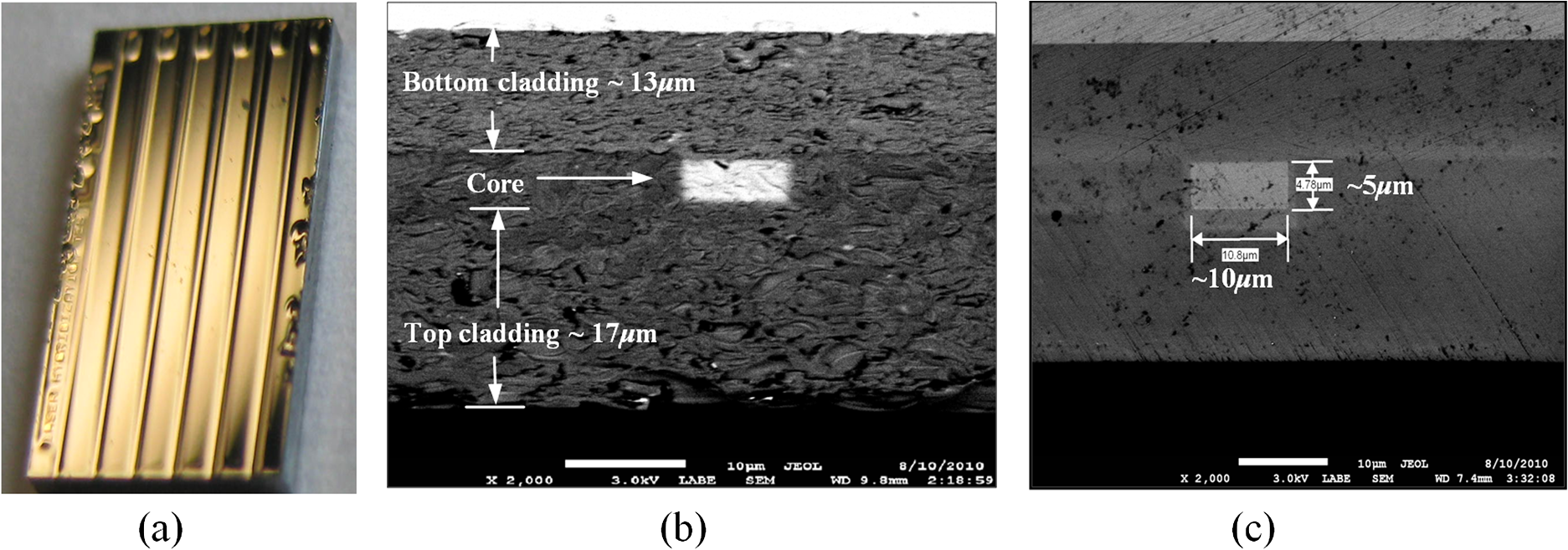
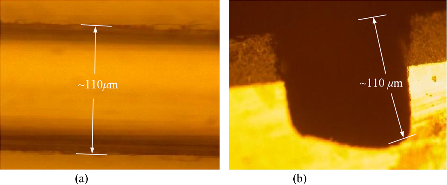
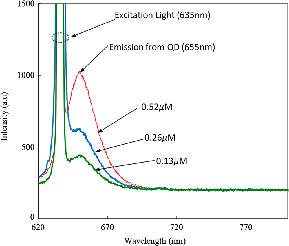
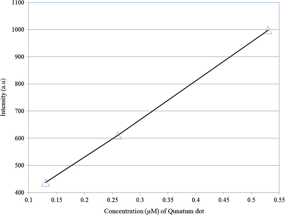
1.IntroductionThe field of Micro Total Analysis Systems (TAS), or Lab-on-a-chip (LOC), has gained increased attention since its introduction by Manz et al.1 in 1990. This is because of several advantages: TAS perform bioanalysis and detection with higher sensitivity by using small amount of reagent volumes in short time. Typically, a bioanalytical process includes sampling, filtration, dilution, chemical reaction, separation, detection and quantification of molecules of interest. To perform all of these processes at micron scale, different process modules need to be miniaturized and integrated in a single chip. Adaptation of conventional micro fabrication technologies for the integration of TAS is complicated and crucial. Several innovative approaches are reported for the integration of micro total analysis systems.2–4 Hybrid integration of TAS using different material platforms such as silicon and glass, and polymeric materials such as polydimethylsiloxane (PDMS), poly (methyl methacrylate) (PMMA), and SU-85–9 are also reported. The main benefit of hybrid integration of TAS is that the properties of different materials can be exploited for supporting different functionalities of TAS. However, the fabrication process can be expensive and complex. Even though many detection techniques are reported for the bioanalytical process, fluorescent detection is still a widely used approach,10 as this method has many advantages including higher sensitivity, better stability, better spatial resolution, and high discrimination capability. Conventionally, fluorescent dyes or fluorescent proteins are used as diagnostic tool in immunoassays.11 Fluorescent dyes are compatible for tagging with the biomolecules and detecting via photoluminescence properties. Emergence of quantum dots (QDs) replaces conventional dyes in immunoassays, due to the enhanced fluorescence, narrow emission and wide absorption spectral width, greater stability against the photo bing, water solubility, and biocompatibility. A review article by Mattoussi et al.12 furnishes a detailed table of advantages of QDs over the fluorescent dye molecules for the biodetection. Miniaturized opto-fluidics biochips, together with highly efficient fluorescent probes, can facilitate bedside testing in hospital with small amounts of sample volume and enhanced sensitivity. However, a major drawback of the optical detection is the complexities involved in building an optical setup with a microfluidic channel. In this context, an increasing demand exists for the simpler, accurate and inexpensive methods of integration of optical microfluidic systems. A simpler approach of fabricating the optical detection module in TAS is to integrate optical fibers directly into microfluidic channels.13 Such systems are not compatible for integrating more optical components and fabricating portable devices. Moreover, they suffer the serious problem of misalignment of fibers with the microchannel. Fabrication of microfludics and optical components using single material platform is a highly useful approach for the realization of portable and robust TAS. For such a monolithic integration of optical waveguides, the materials with better transparency to the wavelength of operation and feasibility of modifying the optical properties, such as refractive index, are essential. For a waveguide, light is confined and propagated through a medium called “core,” which is buried inside a cladding medium. The refractive index of the core must be slightly greater than the cladding to satisfy the condition of total internal reflection at the core-cladding interface and, hence, the light is guided through the core. The fabrication of microfluidic components requires the patterning of material into complex 3D high-aspect ratio structures; also, they must be sealable with a strong leak-proof bonding. Therefore, the materials possessing all of the above stated properties are required for the monolithic integration of optical microfluidic systems. PDMS is identified as a suitable material for fabricating TAS because of several advantages: it is bio-compatible, optically transparent down to the UV range (making it attractive to fabricate optical components), and easily moldable to any complex 3D microstructures by soft lithography which is a low cost fabrication process. Chang-Yen et al.14 report an attempt of developing waveguides and microfluidics monolithically on PDMS. The refractive index requirements of core and cladding of waveguide is achieved by modifying the curing temperature of the PDMS. The complexity in the proposed process is that the curing of core and cladding must be done separately, as the refractive index of PDMS is dependent on the curing temperature. The attenuation of the PDMS waveguide was , which is several orders higher than that of a SOS waveguide. The loss of the SOS waveguide is reported as low as .15 The SOS platform is proven to be suitable for the miniaturization of monolithic-analytical systems.16,17 In SOS platform, silicon dioxide layers are deposited and micro-machined on silicon substrate for realizing the photonic components. The refractive index of the silica layers can be easily modified by varying the process parameters; therefore, the micro-optical components such as waveguide, couplers, and grating based spectrometers18 can be fabricated. SOS is an interesting technology in the optical point of view, as the existing, well-characterized semiconductor processing technologies can be readily adopted for the deposition of high-quality oxide films. Since the optical absorption is very low for the silicon dioxide throughout the entire UV through near infrared regions, low-loss optical components can be fabricated on it. The microfluidic components such as microchannels, reaction chambers, and optical components can be monolithically integrated on SOS platform without any mis-alignment issues. However, the fabrication issues reported in the literatures are deep micromachining of the silicon dioxide and hermetic sealing of the microfluidics circuits due to the non-planar topology of the waveguide. As mentioned, the fabrication of optical components on SOS platform requires deposition, photo-patterning, and anisotropic etching of silicon dioxide layers. To minimize the optical loss, the roughness of the etched-surface and verticality of the structures should be given more attention. In addition, the core layer needs to be deeply buried, typically 15 to 20 μm within the cladding layers. Therefore, the silica layer must be deeply etched (more than 20 μm) to bring the microfluidics to the optical path. Technologies such as deep reactive ion etching (DRIE)19,20 and laser machining21 are reported for the high-aspect ratio micromachining of silica layer, but they are expensive, complex, and time consuming. Recently, a low-cost, nontraditional micromachining technology called spark assisted chemical engraving (SACE)22 has been employed for the machining of silica layer deposited on silicon substrate. Development of microfluidic channel and optical waveguide on SOS using SACE is still underway, due to high roughness surface associated with the SACE. Laszle et al.23 report a method of making microchannel on glass by diamond sawing, which is simple and can be carried out in a general laboratory environment. Even though this technique is suitable for fabricating straight microchannels, the machined-surface can be very rough. In this work, a novel optical microfluidic system is developed by integrating SOS waveguide on PDMS. Advantages of PDMS for the microfluidics circuits, and SOS for the optical waveguide, are exploited in this work. Due to the fabrication complexities and the higher attenuation of PDMS waveguide, SOS waveguide is used. In the proposed integration method, by using two simple technologies, an optical microfluidic system is implemented using SOS waveguides and PDMS microfluidic chips. The diamond micromachining method is used for the fabrication of a straight microfluidic channel in SOS waveguide, which is a simple and cost-effective method. However, to have a fluidic system, the SOS chip is further integrated on a PDMS platform containing more microfluidics components. The microfluidic structures requiring high aspect-ratio were easily fabricated on PDMS by soft lithography, which can be carried out in a general laboratory environment. The easily sealable nature of PDMS, with PDMS or glass, is exploited for the sealing of devices using oxygen plasma treatment. The use of thin PDMS layer for the sealing of devices could solve fabrications issues due non-planar topology of the waveguide. The use of diamond machining, together with the integration on PDMS, made the fabrication of optical TAS an easy and cost-effective process. Diamond machining always results in a surface with high roughness which reduces the optical coupling efficiency between the waveguide and microfluidics. Hence, a new chemical polishing facility called CP (microfluidics-assisted chemical polishing) was developed to improve the surface roughness. The proposed integration method broadens the feasibilities of fabricating optical TAS comprised of any complex microfludic systems such as separation systems, micromixers, and micropumps on PDMS, followed by integrating SOS waveguide with a straight microchannel for the optical detection requirements. The roughness of the channel wall introduced from the diamond machining is smoothed by CP. 2.SOS-PDMS Optical-Microfluidic SystemFigure 1(a) shows the schematic illustration of the SOS-PDMS integration process. This process is designed to implement an optical microfluidic system by using simple, easy, and low-cost fabrication processes. Also, the process of integration of SOS and PDMS is designed to be carried out in a general laboratory environment. As the optical property of the waveguide is very sensitive to the fabrication process and to the quality of micromachining such as surface roughness and verticality of the structures, the fabrication of waveguide was carried out in a standard microfabrication facility. The microfluidic circuits on SOS platforms demands deep machining of silicon dioxide, which is an expensive and tedious task in a standard semiconductor fabrication facility. Therefore, the integration of microfluidics on SOS waveguide was achieved using the advantages of SOS and PDMS platforms, as demonstrated in Fig. 1(a). The assembly consists of two chips: one is the microfluidics chip on PDMS, and the other is the microfluidics channel-integrated optical waveguide on SOS platform. The PDMS platform is pattered by the soft lithography. This microfluidic platform contains a slot for fixing the SOS chip, liquid reservoirs, a microchannel, and a region where fluid is injected into the microfluidic channel on the SOS chip (fluidic injection zone). The SOS chip with a straight microchannel [Fig. 1(b)] must be properly aligned with the microchannel in PDMS while bonding. Fig. 1(a) Schematic illustration of silica-on-silicon-PDMS optical-microfluidic system and (b) SOS waveguide with a straight microchannel.  Two fabrication issues are considered while designing this integration process: sealing of the SOS waveguide with non-planar topology of waveguide and the alignment of the microchannel in the waveguide and the PDMS platform. In this process, the bonding of the device was done using oxygen plasma treatment. One main issue with the oxygen plasma bonding is that plasma-treated substrates must be immediately bonded without contaminating them. At the same time, the microchannels in the SOS chip and the PDMS platform must be carefully aligned. To solve this issue, the fluid injection zone is designed by chamfering the microchannel ends, as shown in Fig. 1(a). After bonding the SOS chip in the slot of PDMS, a thin layer of PDMS is used to seal the device. This thin PDMS layer is sufficiently flexible to fill all the non-planar regions of the waveguide and produce a leak-proof hermetical sealing. 3.Silica-on-Silicon WaveguideIn SOS technology, wave guiding is achieved by three layers of silicon dioxide—namely bottom cladding, core, and top cladding layers deposited on the silicon substrate. By choosing for the core a slightly higher refractive index than the cladding layer, the light can be vertically confined in the core. For the lateral confinement, the core layer must be structured to the desired width. After structuring the core layer, the top cladding layer of silicon dioxide is deposited in a buried core waveguide structure. An illustration of crossectional view of SOS waveguide is shown in Fig. 2. Since the topology of the waveguide is non-planar, sealing the microfluidic channels integrated on the SOS waveguide is a challenging task. Among the few techniques reported for the planarization of the waveguide topology, chemical mechanical planarization (CMP) and etch back method are usually employed for the hermetic sealing of the microfluidic components machined on the SOS waveguide. In CMP, many parameters must be carefully controlled to obtain a reproducible outcome as the CMP is a combination of mechanical abrasion and chemical reaction.24 Even though many commercial tools are available for the CMP to precisely control the process parameters, they still suffer from issues such as feature-size-dependent polishing, hollow formation in wide features, and residual contamination. Etch back method is a technique used in microelectronics fabrication process for the planarization of small unevenness (), which is not suitable for the present configuration. To adopt this technique for the waveguides, for the unevenness of , etching with two sacrificial layers is also reported.25 Ruano et al.26 reported monolithic integration of waveguide and microfluidic system including microchannel and liquid reservoirs by depositing glass using flame hydrolysis deposition (FHD) and etching with deep reactive ion etching (DRIE), followed by sealing the device with the help of two PDMS layers. Herein, to get a hermetic sealing, a thin flexible PDMS layer is bonded between the nonplanar waveguide and a thick PDMS layer containing the fluidic ports. This kind of double layer sealing is required since all the fluidic parts including the liquid reservoirs and microchannels were monolithically integrated on the waveguide; therefore, the sealing layer should be sufficiently thicker and less flexible to fix the fluidic ports. In our work, the proposed SOS-PDMS integration greatly simplifies the issues with the sealing of the microfluidic channel. The main advantage of our method is that any complex 3D microfluidic components required for separation, mixing, and micropumping can be patterned on PDMS by soft lithography and integrated with SOS chip with a straight microfluidic channel to facilitate the realization of complex optical-LOCs through an easy and inexpensive process. 4.Device Fabrication and Integration4.1.Fabrication of SOS Chip with Waveguide and MicrofluidicsThe fabrication of SOS waveguide is carried out in a standard clean room facility. The waveguide fabrication starts with the deposition of a silicon dioxide layer on the silicon wafer ((100) orientation) by Plasma Enhanced Chemical Vapor Deposition (PECVD). A PlasmaLab 80 Plus instrument is used for the PECVD of silicon dioxide. For the bottom cladding layer, the chamber was evacuated to 1000 mTorr and heated to 300°C, subsequently the mixture of silane and nitrogen (5 percent , 95 percent ) at the flow rate of 170 sccm; nitrous oxide () at the flow rate of 710 sccm were introduced to the chamber. The plasma was created by the RF power of 20 W at 13.56 MHz. The deposition carried out for 4 h and 30 min, and resulted in a 13 µm-thick bottom cladding layer on the silicon. The refractive index of the bottom cladding layer was measured at using ellipsometry. For the core, to achieve higher refractive index than the cladding layer, flow rate of the silane-nitrogen mixture was increased to 500 sccm and RF power was increased to 200 W. The deposition rate of the process was . Hence, the deposition was carried out for 40 min to obtain the thickness of 5 μm. The refractive index of the core layer was measured at 1.457. For structuring the core layer (10 μm width) of the waveguide, photo resist masking layer was patterned by using UV photolithography. MERIE P5000 plasma machine of applied materials was used for the RIE of core layer. Finally, the top cladding layer was deposited with the process, as that of the parameters of the bottom cladding layer for 5 h. Due to the conformal deposition of the top cladding layer on the patterned core layer, an unevenness of around 5 μm was observed on the thickness of the waveguide. Finally, the waveguide was diced into samples, as shown in Fig. 3(a). Each chip has six waveguides of core crosssections, separated by 500 μm. The waveguide facets were polished using diamond lapping film of 0.1 μm particle size (Allied High tech, California, USA) to enhance the coupling of light to the waveguide. To assess the quality of the waveguide facet, the facets were imaged by FEG-SEM. Figures 3(b) and (3c) show the SEM image of waveguide before and after polishing, respectively. The dimensions of the core and cladding are clearly visible in the SEM photo. 4.2.Diamond Micromachining of the MicrochannelEsec 8003 dicing saw was used for the fabrication of microchannel on SOS waveguide. This machine was designed to cut semiconductor wafers into chips. The blade used in the setup is a steel ring with diamond particles the size of 5 μm coated on it. The thickness of the blade was 100 μm. The blade was mounted on a high-frequency air-bearing spindle. The rotation speed of the wheel was set at 18000 rpm. The sample was fixed to the vacuum check by using a UV curable tape, the thickness of 80 μm. A height sensor is used in the setup to measure the height of the diamond saw from the chuck. The height of the blade was set to 540 μm to have a channel depth of (). The machining speed was set to 1 mm/s. Figure 4 shows the microscope image of the microfluidic channel fabricated on the SOS chip. The width and depth of the channel was measured by using an optical microscope, and they were . 4.3.PDMS Microfluidic PlatformThe PDMS platform contains a slot for fixing the SOS chip, microfluidic channel and liquid reservoirs. The depth of the slot for fixing the SOS chip was 560 µm. The depth of the microfluidic channel in the PDMS was 80 µm. The mold for the PDMS platform was designed in commercial software called ProEngineer, PTC, Needham, USA and fabricated on brass by CNC machining. A thin layer of gold was electroplated on the brass mold for the easy removal of PDMS. Soft lithography for the fabrication of PDMS platform is carried out in a general laboratory environment. PDMS platform is fabricated by a two-component silicone elastomer kit which is SYLGARD 184 obtained from the Dow Corning, MIDLAND MI, USA. The silicon base and curing agent (crosslinker) are mixed in 10:1 (wt.%) ratio. This mixture contains air bubbles generated from the mixing; hence the mixture was placed in a vacuum desiccator and degassed until all the gas bubbles were removed. Furthermore, PDMS was casted on the brass mold and baked at 80 °C for 5 h. The baking temperature or time is not critical, as the optical property of the PDMS, such as the refractive index, is not a concern in the present work. The crosslinking time can be decreased by increasing the curing temperature. Figure 5 shows the brass mold and the PDMS platform fabricated by soft lithography. 4.4.Integration of PDMS and SOS ChipOnce the PDMS platform is fabricated, the next step is the integration of a SOS chip. The device fabrication involves two bonding process: first, the bonding of SOS chip on the slot of the PDMS platform, and second, the sealing of the microfluidics channel by a thin layer of PDMS. Finally the fluid inlet and outlet tubes must be interconnected on top of the liquid reservoirs. Oxygen plasma treatment was used for the bonding of the device. The exposure of oxygen plasma on the PDMS surface helps to clean the surface, together with the modification of hydrophobic nature of PDMS to the hydrophilic by converting the -unit in PDMS to silanol group (). The quality of the bond is determined by the exposure time and how quickly the samples are kept in contact after the exposure and before contaminating and losing the surface property. If an aligning task is involved in the bonding, the bonding process requires extensive care and expertise. The plasma exposure is carried out in the instrument obtained from Harrick plasma. For the first bonding process of device fabrication, the back side of the SOS chip (with the silicon surface) and PDMS platform are washed in deionized (DI) water and dried with an air gun and loaded into the plasma instrument. The plasma chamber pressure was pumped down to 70 mTorr and the oxygen was introduced at 10 sccm into the chamber. The plasma was created by RF power. The samples were exposed to the oxygen plasma for 35 s. The SOS chip was placed in the slot on PDMS and pressed. The region of transition of channel in PDMS to SOS chip is designed by chamfering the channel ends to eliminate the misalignment problem between the microfluidic channel in PDMS and the SOS chip, resulting in no alignment issue due to the present bonding process. This bonding process immediately forms a strong leak proof bond of chip on PDMS. The next step of device fabrication is the sealing of the device. A thin flat layer of PDMS with the thickness of 2 mm is used for sealing the device. The same process of preparation of PDMS explained before is used for the thin PDMS layer also; herein, the PDMS was casted on a silicon wafer to obtain a flat layer. Before casting the PDMS, the silicon wafer was silanized with a vapor of trichlorosilane in a covered Petri dish on a hot plate at 55 °C for 5 h for promoting the easy removal of the PDMS. The wafer was placed in a Petri dish and poured the PDMS and baked at 80 °C for 3 h. Then the PDMS layer was peeled off from the wafer and cut into samples. Two holes at 2 mm diameter were punched to insert the fluidic tubes. The position of the holes on the PDMS layer is on the position of liquid reservoirs in the PDMS platform. The PDMS platform with the SOS chip and the thin flat layer were cleaned in DI water and exposed to the oxygen plasmas, as explained earlier. The samples were pressed with the elapse of no time. This process yields a hermetic and irreversible sealing of microfluidic channels. The fluidic tube (obtained from Gilson Mandel, Middleton WI, USA) with an inner diameter of 250 µm and outer diameter of 2 mm, was inserted into the hole punched on the PDMS layer and glued with a one-component silicon RTV adhesive obtained from the Dow Corning. This adhesive was selected to be highly viscous so that, before the completion of heating and curing, it does not reach the liquid reservoirs and blocks the microfluic channel. The sample was cured in the oven at 100 °C for 1 h. Figure 6(a) shows the photograph of the fully integrated SOS-PDMS LOC. Fig. 6(a) SOS-PDMS Lab-on-chip and (b) close up of the flow in transition microfluidic zone between SOS and PDMS chip.  The device was tested with microflows to test for the flow behavior and the possible leakages. Initially, DI water was pumped by Minipuls™, Gilson, Middleton WI, USA 3 peristaltic pump. The inlet velocity was varied slowly from 0.05 to and no leakage was noticed. To test the flow behavior through the device, DI water containing the polystyrene spheres of 5 µm size, purchased from the Duke Scientific (No.G0500), was used. The polystyrene spheres were dispersed in DI water at a volume fraction of and pumped through the device. The pumping was done under a microscope (Nikon ECLIPSE 80i, Melville, NY, USA) to image flow pattern. Figure 6(b) shows the flow through the fluidic injection zone imaged under the microscope, herein the inlet velocity was set at . The flow stream line imaged with the help of polystyrene spheres showed that when the inlet velocity was increased to , two fluidic stagnation areas were observed in the two corners of the fluid injection zone. When the fluidic was pumped below the , the stagnation area was reduced to the extreme corners of the fluidic injection zone, as shown in Fig. 6(b). The liquid stagnation in the fluidic path is not favorable during the rinsing of the channel, as it can accumulate the chemical wastes in the chip and results in errors in the measurements. Therefore, the cleaning of the channel after each measurement was done at a slower velocity. Since the integration of the microchannel in SOS waveguide was done by diamond machining, the surface quality of the channel wall needed further surface finishing so that the light coupling between the waveguide and the microfluidic channel was not affected. The quality of coupling of the excitation light to the microfluidic channel, and the collection of the fluorescent light from the channel, can be reduced significantly by the roughness of the channel wall. The channel wall surfaces were polished by microfluidic-assisted chemical polishing (CP). A commonly used silicon dioxide etchant which is buffered hydrofluoric acid (BHF) was pumped through the channel for polishing the channel wall. BHF was prepared from HF and ammonium fluoride in ratios. The stability of PDMS in BHF was tested before pumping the BHF to the device. Several PDMS samples with microstructures were soaked in the BHF different times and the microstructures were slightly deformed after about 15 min of soaking. Hence, in the case of CP, BHF was pumped through the microchannel fabricated in SOS chip for 10 min at velocity to reduce the surface roughness of the microchannel wall fabricated by diamond machining. 4.4.1.Optical Measurement SetupA fiber-to-waveguide aligner setup was built for the fluorescence detection. Figure 7 shows the setup used for the fluorescence detection experiments. This setup includes two high-precision micropositioners, fiber chucks and fiber holders obtained from Newport, Irvine CA, USA. Micropositioners are five-axes controllable. Light from a fiber laser (OZ Optics, Ottawa, Canada, 635 nm, 5 mW) was directly coupled to the waveguide with the help of opto-mechanical setup. A multimode fiber is aligned with the waveguide for collecting the florescence signal and coupling to the spectrometer. A commercially available spectrometer (Ocean Optics, USB 4000, Dunedin, USA) was used for the fluorescence measurements. 5.Results and DiscussionFluorescence is one of the preferred ways of biodetection in many bioassays and other LOCs. Quantum dots (QDs) have many advantages over fluorophores such as narrow emission peak, wide absorption band and good stability. As the QDs are used in many biodetection applications such as the detection of protein toxins (staphylococcal enterotoxin B, cholera toxin),27 ricin, shiga-like toxin 1 (SLT), staphylococcal enterotoxin B (SEB),28 Escherichia coli and Salmonella typhimurium29 and the detection of single-nucleotide polymorphism in human oncogene p53, and for the multiallele detection of viruses like hepatitis and the hepatitis 30 the proposed LOC is demonstrated for the detection of fluorescence from QD to show the possibility for many bio-applications. For the investigation of fluorescence detection capability of the SOS-PDMS LOC, QD655 was used. QD 655 can be exited with any wavelengths below 650 nm, and it produces a narrow emission peak at 655 nm. QD 655 was obtained from Invitrogen Company, and is used as received. QD 655 was suspended in 50 mM borate buffer. QD655 was further diluted to different concentrations in DI water for investigating the detection limit of the device. Figure 8 shows the spectra of the fluorescence emission from QD 655 recorded from the device. The QD solution was pumped to the microchannel of the device and excited by laser light of 635 nm, coupled to the microchannel through the fiber and SOS waveguide. A collection fiber was aligned at the other end of the SOS waveguide to couple the fluorescence light to the spectrometer. Since no filter is used for removing the excitation signal, two peaks are visible in Fig. 8: one at 635 nm that corresponds to the excitation light, and the other at 655 nm that corresponds to the emission from quantum dots. The three spectra in Fig. 8 correspond to emissions from three different concentrations of the QD. After taking the measurements for each concentration, the device was cleaned by pumping DI water for 3 min. From Figs. 3(b) and 4(b), we know that the core of the waveguide is located above the silicon surface and the depth of the microchannel is . This means the waveguide is located at the microchannel, and only a portion of the sample flowing through the microchannel is detected. Hence, if an air bubble stays on top portion of the channel, the device cannot detect the signal correctly. To confirm no air bubbles are trapped, each measurement is repeated several times by pumping the solution through the microchannel, and recording the measurements. The detection limit of the device is found to be as low as 0.13 µM. A graph plotted between the fluorescence intensity recorded in the spectrometer for each concentration of QD is shown in Fig. 9. As can be seen in Fig. 9, a linear variation between the fluorescence and concentration of QDs is observed. This experiment demonstrates that the proposed LOC can be used for many bio-applications based on QD fluorescence detection. 6.ConclusionA new method of integrating an optical microfluidic system by using SOS-based microphotonics chip and PDMS-based microfluidic chip is proposed. Two simple and low-cost technologies, namely diamond micromachining and soft lithography, were used for the fabrication of the device. By exploiting the benefits of PDMS for fabricating high-aspect ratio microfluidic structures together, with the integration of low-loss SOS photonics waveguides, greatly simplifies the fabrication of optical micro total analysis systems. Furthermore, the optical loss from the roughness of the channel wall introduced by the diamond machining was minimized by the microfluidic assisted chemical polishing of the channel wall to obtain the optical coupling between waveguide and microfluidic channels. The performance of the device was tested by detecting the laser-induced fluorescence from QDs of different concentrations. The detection limit of the present device was found as low as 0.13 µM for QDs 655. Thus, the proposed SOS-PDMS integration demonstrates the possibility of realizing simple and less-expensive LOCs for bio-detection based on QD fluorescence. AcknowledgmentsThe authors thank the financial support of the Canadian Institute for Photonics Innovations and NSERC and technical support of the Enablence Technologies, Inc., Ottawa, Canada. ReferencesA. ManzN. GraberH. M. Widmer,
“Miniaturized total chemical analysis systems: a novel concept for chemical sensing,”
Sensors Actuat. B. Chem., 1
(1–6), 244
–248
(1990). http://dx.doi.org/10.1016/0925-4005(90)80209-I SABCEB 0925-4005 Google Scholar
D. R. Reyeset al.,
“Micro total analysis systems. 1. Introduction, theory, and technology,”
Anal. Chem., 74
(12), 2623
–2636
(2002). http://dx.doi.org/10.1021/ac0202435 ANCHAM 0003-2700 Google Scholar
P. A. Aurouxet al.,
“Micro total analysis systems. 2. Analytical standard operations and applications,”
Anal. Chem., 74
(12), 2637
–2652
(2002). http://dx.doi.org/10.1021/ac020239t ANCHAM 0003-2700 Google Scholar
T. VilknerD. JanasekA. Manz,
“Micro total analysis systems recent developments,”
Anal. Chem., 76
(12), 3373
–3386
(2004). http://dx.doi.org/10.1021/ac040063q ANCHAM 0003-2700 Google Scholar
K. B. MogensenJ. El-AliA. WolffJ. P. Kutter,
“Integration of polymer waveguides for optical detection in microfabricated chemical analysis systems,”
Appl. Opt., 42
(19), 4072
–4079
(2003). http://dx.doi.org/10.1364/AO.42.004072 APOPAI 0003-6935 Google Scholar
H. Satoet al.,
“An all SU-8 microfluidic chip with built-in 3D fine microstructures,”
J. Micromech. Microeng., 16
(11), 2318
–2322
(2006). http://dx.doi.org/10.1088/0960-1317/16/11/010 JMMIEZ 0960-1317 Google Scholar
G. S. FioriniD. T. Chiu,
“Disposable microfluidic devices: fabrication, function, and application,”
BioTechniques, 38
(3), 429
–446
(2005). http://dx.doi.org/10.2144/05383RV02 BTNQDO 0736-6205 Google Scholar
R. Palet al.,
“An integrated microfluidic device for influenza and other genetic analyses,”
Lab. Chip, 5
(10), 1024
–1032
(2005). http://dx.doi.org/10.1039/b505994a LCAHAM 1473-0197 Google Scholar
P. de la Fuenteet al.,
“A SU-8 microfluidic total analysis system integrating silicon photodiodes and buried waveguides,”
in Electron Devices, 2005 Spanish Conference,
461
–464
(2005). Google Scholar
S. GötzU. Karst,
“Recent developments in optical detection methods for microchipseparations,”
Anal. Bioanal. Chem., 387
(1), 183
–192
(2007). http://dx.doi.org/10.1007/s00216-006-0820-8 ABCNBP 1618-2642 Google Scholar
N. P. Voloshinaet al.,
“Alexa dyes, a series of new fluorescent dyes that yield exceptionally bright, photostable conjugates,”
J. Histochem. Cytochem., 47
(9), 1179
–1188
(1999). http://dx.doi.org/10.1177/002215549904700910 JHCYAS 0022-1554 Google Scholar
K. E. Sapsfordet al.,
“Biosensing with luminescent semiconductor QDs,”
Sensors, 6
(8), 925
–953
(2006). http://dx.doi.org/10.3390/s6080925 SNSRES 0746-9462 Google Scholar
A. ChandrasekaranM. Packirisamy,
“Integrated microfluidic biophotonic chip for laser induced fluorescence detection,”
Biomed. Microdev., 12
(5), 923
–933
(2010). http://dx.doi.org/10.1007/s10544-010-9447-9 BMICFC 1387-2176 Google Scholar
D. A. Chang-YenR. K. EichB. K. Gale,
“A monolithic PDMS waveguide system fabricated using soft-lithography techniques,”
J. Lightwave Technol., 23
(6), 2088
–2093
(2005). http://dx.doi.org/10.1109/JLT.2005.849932 JLTEDG 0733-8724 Google Scholar
H. Ou,
“Different index contrast silica-on-silicon waveguides by PECVD,”
Electron. Lett., 39
(2), 212
–213
(2003). http://dx.doi.org/10.1049/el:20030165 ELLEAK 0013-5194 Google Scholar
P. Friiset al.,
“Monolithicintegration of microfluidic channels and optical waveguides in silica on silicon,”
Appl. Opt., 40
(34), 6246
–6251
(2001). http://dx.doi.org/10.1364/AO.40.006246 APOPAI 0003-6935 Google Scholar
J. OzhikandathilM. Packirisamy,
“Silica-on-silicon (SOS)-PDMS platform integrated lab-on-a-chip (LOC) for quantum dot applications,”
Proc. SPIE, 7750 775004
(2010). http://dx.doi.org/10.1117/12.873112 PSISDG 0277-786X Google Scholar
T. AkimotoH. NanbuE. Ikawa,
“Reactive ion etching lag on high rate oxide etching using high density plasma,”
JVSTB: Microelectron. Nanometer Struct., 13
(6), 2390
–2393
(1995). http://dx.doi.org/10.1116/1.588006 JVSTBM 1071-1023 Google Scholar
L. A. Donohueet al.,
“Developments in Si and SiO2etching for MEMS-based optical applications,”
Proc. SPIE, 5347 44
–53
(2004). http://dx.doi.org/10.1117/12.524471 PSISDG 0277-786X Google Scholar
C. Hnatovskyet al.,
“Fabrication of microchannels in glass using focused femtosecond laser radiation and selective chemical etching,”
Appl. Phys. A., 84
(1), 47
–61
(2006). http://dx.doi.org/10.1007/s00339-006-3590-4 APAMFC 0947-8396 Google Scholar
J. Ozhikandathilet al.,
“Low resistive silicon substrate as an etch stop layer for drilling thick SiO2 using spark assisted chemical engraving,”
Microsyst. Technol., 17
(3), 373
–380
(2011). http://dx.doi.org/10.1007/s00542-011-1248-4 MCTCEF 0946-7076 Google Scholar
L. SzekelyR. Freitag,
“Fabrication of a versatile microanalytical system without need for clean room conditions,”
Anal. Chim. Acta, 512
(1), 39
–47
(2004). http://dx.doi.org/10.1016/j.aca.2004.02.016 ACACAM 0003-2670 Google Scholar
K. Achuthanet al.,
“Investigation of pad deformation and conditioning during the CMP of silicon dioxide films,”
J. Electron. Mater., 25
(10), 1628
–1632
(1996). http://dx.doi.org/10.1007/BF02655587 JECMA5 0361-5235 Google Scholar
Y. X. LiP. J. FrenchR. F. Wolffenbuttel,
“Plasma planarization for sensor applications,”
J. MEMS, 4
(3), 132
–138
(1995). http://dx.doi.org/10.1109/84.465122 1057-7157 Google Scholar
J. M. Ruanoet al.,
“Design and fabrication of a silica on silicon integrated optical biochip as a fluorescence microarray platform,”
Biosens. Bioelectron., 18
(2–3), 175
–184
(2003). http://dx.doi.org/10.1016/S0956-5663(02)00170-7 BBIOE4 0956-5663 Google Scholar
E. R. Goldmanet al.,
“Avidin: a natural bridge for quantum dot-antibody conjugates,”
Am. Chem. Soc., 124
(22), 6378
–6382
(2002). http://dx.doi.org/10.1021/ja0125570 JACSAT 0002-7863 Google Scholar
E. R. Goldmanet al.,
“Multiplexed Toxin Analysis Using Four Colors of Quantum Dot Fluororeagents,”
Anal. Chem., 76
(3), 684
–688
(2004). http://dx.doi.org/10.1021/ac035083r ANCHAM 0003-2700 Google Scholar
L. YangY. Li,
“Simultaneous detection of Escherichia coli O157:H7 and Salmonella Typhimurium using quantum dots as fluorescence labels,”
Analyst, 131
(3), 394
–401
(2006). http://dx.doi.org/10.1039/B510888H ANLYAG 0365-4885 Google Scholar
D. Gerionet al.,
“Room-temperature single-nucleotide polymorphism and multiallele DNA detection usingfluorescent nanocrystals and microarrays,”
Anal. Chem., 75
(18), 4766
–4772
(2003). http://dx.doi.org/10.1021/ac034482j ANCHAM 0003-2700 Google Scholar
|