
|
|
1.IntroductionOptogenetic techniques have gained increased attention during the last years because they provide new and powerful means for interacting with biological systems.1 Since the first experiment on optical stimulation of mammalian neurons that were genetically modified to express the light-sensitive protein channelrhodopsin (ChR2),2 there have been many developments in the field. At the biochemical frontier, ChR2s with faster kinetics and reduced inactivation upon subsequent stimulations were discovered.3–5 At the technical frontier, novel devices for delivery of optical stimuli were engineered and applied6 shedding light on important systems in vitro7 and in vivo.8–10 Optical stimulation has several major advantages over electrical stimulation methods. In electrical stimulation, high currents applied to trigger cell depolarization can cause permanent membrane damage. On the contrary, cells stimulated by light are not permeabilized under normal stimulation conditions. In case of excessive photoexposure, desensitization of the photo-sensitive entity might occur, thus, leaving the rest of the cell intact. Another advantage of optical stimulation is given by an improved resolution and spatial control over the stimulated region. When focusing the light pulses to a spot of several microns in size, subcellular stimulation resolution can be achieved.11,12 Although nanotechnology fabrication, in principle, allows the production of extremely small electrical devices, the resolution of a functional stimulation electrode is limited by the charge delivery capacitance at the interface. Thus, to provide sufficient current for extracellular cell depolarization without exceeding the safe stimulation window, the electrodes are typically made in the range of 10 μm diameter or larger. Furthermore, several cells may be depolarized in the vicinity if the induced voltage amplitude exceeds the depolarization threshold. In contrast, light stimulation can be made highly specific to a certain cell type. This is achieved via precise targeting of the cells of interest by using a cell type specific promoter in the plasmid carrying the optogenetic construct. An interesting feature of optical manipulation is the possibility of inhibiting cell activity. For example, the chloride pump halorhodopsin induces hyperpolarization of the cell upon exposure to yellow light, owing to the influx of negatively charged ions inside the cell and, thus, lowering the intracellular potential.13 In addition to manipulation, optical recording is also possible with dyes sensitive to a specific ion which allows real-time monitoring of action-potentials (AP) using microscopic techniques.14 At the other end of electrophysiology, namely recording from electrogenic cells, microelectrode arrays (MEAs) have become a major tool, which complements the patch-clamp technique for the investigation of network activity.15–18 MEAs provide multisite recording capabilities in combination with direct on-chip cell culture. Thus, they facilitate chip-based extracellular recording from networks where many probes are required over the duration of several days to weeks. The combination of optogenetics, light stimulation, and physiological MEA recordings can be employed for bidirectional communication with cells. Recent advances in the field of miniaturized light sources have led to the development of micropixellated arrays of light-emitting diodes (μLEDs) with more than 4000 LEDs in an area of less than (Ref. 19). Such devices have been integrated as versatile light sources into microscopes, thus, allowing further focusing of the projected spots. This approach can deliver high light densities in the range of 30 to at subcellular resolution, which is sufficient for exciting optogenetically modified cells.20–22 The system was successfully utilized for optical stimulation of neuronal cells cultured on MEAs.12,23 The emission wavelength of the μLEDs can be tuned either by the ratio of materials in the InGaN heterostructure or by application of light-shifting polymers that convert typically UV-light into visible wavelengths.24 Therefore, excitation of light-sensitive proteins with diverse absorption spectra is now possible. A particularly interesting aspect of μLEDs is the small lateral dimension of the individual pixel of less than 20 μm.19,25 This provides the possibility of optically addressing individual cells growing on the chip surface without additional optics. Further miniaturization of systems capable of bidirectional optical-electrical communication with cells implies integration of both stimulating and recording units on a single chip. In this work, we have pursued this approach and developed a combined μLED-MEA device capable of direct on-chip optical stimulation as well as extracellular electrical recording. The chips are interfaced, in such a way, that each microelectrode is aligned directly above a single μLED pixel, thus, forming a light spot of to 40 μm at the chip’s surface. Individual μLEDs and microelectrodes can be addressed independently. Optogentically modified cells are cultured directly on the chip and depolarization is induced upon illumination with blue light coming from the μLED array. Triggered APs can be recorded via planar metal microelectrodes that are located beneath the cells in the form of capacitively coupled voltage transients. A schematic of the coupled μLED-MEA device, and its proposed working mode, is shown in Fig. 1. Fig. 1Schematic image of the micropixellated light-emitting diode (μLED)-microelectrode array (MEA) chip design (not to scale). Individual colors signify the material indicated throughout. Single μLED pixel on a sapphire substrate with gold -contacts additionally passivated with a layer, and one of the 64 microelectrodes of a MEA on quartz () substrate glued with PMMA. Blue light excitation depolarizes a transfected HL-1 cell expressing channelrhodopsin (ChR2) proteins sitting on top of the microelectrode. An action potential (AP) is recorded via capacitive coupling to the electrode. 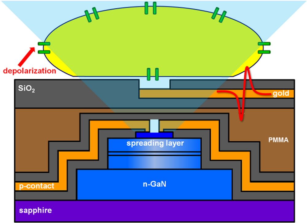 2.Experimental Section2.1.ChemicalsPolydimethylsiloxane (PDMS, Sylgard® 184) was obtained from Dow Corning GmbH (Wiesbaden, Germany). A mixture of elastomer and curing agent in a ratio of was prepared and stored in a freezer at before use. Medical epoxy resin (302-3M) was purchased from Epoxy Technology (Billerica, Massachusetts). Claycomb medium, penicillin-streptomycin (Pen/Strep) mixture, norepinephrine, -glutamine, and laminin were obtained from Sigma (St. Louis, Missouri) and fetal bovine serum (FBS), Fura-2 were obtained from Invitrogen (Darmstad, Germany) and used without further purification. Electrofection experiments were performed using an Amaxa™ Rat Neuron Nucleofector™ Kit from Lonza (Lonza Cologne GmbH, Cologne, Germany). 2.2.Fabrication of Micropixellated Light-Emitting DiodesThe detailed fabrication process of the micropixellated light-emitting devices has been described previously.19,26 Briefly, standard metal–organic chemical-vapor deposition-grown LED wafers, with emission wavelength of 470 nm (blue), were used for device fabrication. The fabrication consisted of six photolithographic steps. First, GaN mesa (row) was defined by inductively coupled plasma (ICP) etching. Then, single pixels with circular disk geometry were also defined by ICP etching. The total diameter of individual pixel was 32 μm, the emission diameter 16 μm, and the inter-pixel spacing 50 μm. In the next step, Ni/Au metal stack () was thermally evaporated and formed the spreading layer. Afterwards, another metal stack was sputtered (Ti/Au, ) and 4 μm wide -contact metal lines, as well as a ring-shaped contacts on the spreading layer, were defined. To act as an isolation layer, a 200 nm layer was deposited onto the surface. In the following step, using reactive ion etching (RIE), the -contact pads and the ring-shaped contacts on top of the spreading layer were open. Finally, a Ti/Au metal stack () was sputtered and patterned to form the interconnection lines for each pixel. An additional step was introduced to ensure mechanical protection of the -contact during the following postprocess, thus, coupling the MEA to the μLED device. An isolating 200 nm layer covering the entire chip surface was deposited using plasma-enhanced chemical vapor deposition (PECVD). The - and -contact openings were defined with electron beam lithography using polymethylmethacrylate (PMMA) resist and subsequent RIE. 2.3.Fabrication of Microelectrode ArraysThe MEAs were fabricated in the clean room using standard microfabrication technologies. Briefly, ultrathin 1-in. quartz wafers (Universitywafer, South Boston, Massachusetts) of 50, 100 or 180 μm thickness were used as a substrate. First, a double layer resist (LOR 3b, Microchem, Newton, Massachusetts and AZ® nLOF 2070, MicroChemicals, Ulm, Germany) was spin-coated onto the wafer and the electrode and feedline geometries were patterned using standard photolithographic procedures. The MEAs consisted of 64 microelectrodes (3 or 6 μm in diameter) with an inter-electrode spacing of 200 μm [Fig. 2(a)]. A stack of metal layers (Ti/Pt/Ti, ) was deposited by electron-beam deposition. Electrodes and feedlines were defined by lift-off. The metal feedlines of the microelectrodes were confined to a width of 8 μm at the edges to block as little light as possible from the 16 μm diameter light-emitting area of the μLED [Fig. 2(b)]. Subsequently, the chip was passivated with a stack of five alternating (200 nm) and (100 nm) layers (ONONO) by PECVD. ONONO was chosen to improve the passivation of the feedlines from the electrolyte solution by decreasing stress and lowering the number of pinholes. A second lithography was performed to remove the passivation layer at the contact pads and microelectrode positions. The ONONO stack was etched down to the platinum layer by RIE using followed by an etch to remove the Ti adhesion layer and possible resist residues. Individual MEAs were diced into chips in order to fit on top of the μLED devices without blocking their - and -contact pads. Fig. 2(a) 64-Channel MEA with 3 μm microelectrodes, scale bar 400 μm. (b) A zoom onto a single microelectrode of 6 μm diameter, scale bar 20 μm. (c–e) μLED chip in different magnifications, scale bars 500, 200, and 100 μm, respectively. (f) Combined μLED-MEA chip with 64 microelectrodes and 841 individually addressable μLEDs, scale bar 1 mm. (g, h) μLED-MEA with switched on LEDs with the focal plane at the μLED and the MEA chip surface, respectively. Pixel bias voltage . Scale bars 400 μm. 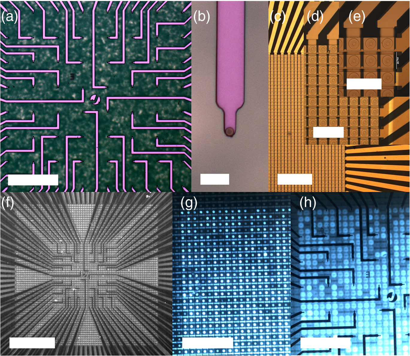 2.4.Fabrication of the Combined μLED-MEA DeviceIn long-term cell culture applications, the protecting passivation layer of MEAs and other functional devices can be negatively affected due to the prolonged exposure to the cell culture medium.27 Hence, a modular concept was applied for the coupling of the μLED to the MEA chip to avoid irrecoverable degradation of the complete μLED-MEA device. The μLED chip was fixed permanently onto a carrier, bonded and passivated, after which, it was well protected and could not be damaged mechanically. At the same time, the MEA chips, which can suffer degradation after prolonged use in ionic cell culture medium, were interchangeable. That is, one μLED device could be reused with different MEA chips. In detail, the μLED chip was first fixed onto a 144 pin chip carrier (CPG14433, Spectrum Semiconductor Material Inc., San Jose, California) using medical epoxy resin and cured at 150°C for 1 h. Subsequently, the - and -contacts were wire-bonded using a wedge bonder and aluminum wire. Overall, 29 -contacts and 29 -contacts (out of 64 available) were connected forming an area of with 841 individually addressable μLEDs. This ensured that, later, the active electrodes on the MEA chip, as well as spaces between the electrodes, could be illuminated at any chosen location. The number of recording sites (64 microelectrodes) is an order of magnitude lower compared to the number of addressable stimulation sites. In principle, the electrode number can be increased. However, the density of high-quality microelectrodes is limited due to the difficulty of integrating a very large number of feed lines on the transparent substrate without the use of multilayer CMOS technology. The central area of the μLED, and the chip carrier pins reserved for later wiring the MEA, were blocked with polyolefine plastomer (POP, Affinity VP8770, Dow, Schwalbach, Germany) and heated to 200°C to ensure good coverage of the blocked areas. Afterwards, the unblocked area of the carrier was covered with epoxy resin, including the wire bonds of the μLED chip, and cured at 150°C for 1 h. After a 5 min soak in 100% ethanol, POP could be easily removed, thus, exposing the area not covered with epoxy resin. Then, the back of the MEA chip was spin-coated with PMMA at 3000 rpm for 1 min, resulting in a 1 μm thick layer (PMMA was easily dissolvable with acetone for future interchange of the MEA chip), placed on top of the μLED chip with micrometer precision using a Fineplacer® (Finetech, Berlin, Germany), and cured at 150°C for 1 h. Later, all 64 electrodes of the MEA were wire-bonded to the carrier which resulted in a active electrode area. A glass ring with a 5 mm diameter and a height of 1 mm was glued to the center of the MEA chip using PDMS. Another ring (diameter 28 mm, height 2 mm) was glued on top of the chip carrier. As a last step, the area between the two rings was filled with PDMS and cured at 150°C for 1 h, thus, forming a 1 mL reservoir for cell culture. Figure 2 demonstrates single parts of the combined chip as well as the complete device with switched on μLEDs. 2.5.Optogenetic Modification of CellsThe cells were cultured and transfected as previously described.28 To summarize, cardiomyocyte-like cell line (HL-1) cells were transfected with a modified CH2-K315-YFP plasmid containing the human Ubiquitin C promoter from Matsuda & Cepko 104 bases ahead of the Ch2 coding sequence, plasmid CMV_Ubi_Ch2_YFP. The YFP fluorescent tag has an emission peak around 527 nm.29 The absorption peak of the rhodopsin molecule in the ChR2 protein is 450 nm.3 The HL-1 cell line30 was derived from AT-1 cells (a mouse cardiomyocyte tumor) by Louisiana State University Health Science Center, New Orleans, LA, USA. It represents a hybrid between embryonic and adult myocytes. The HL-1 cardiac muscle cells show spontaneous APs, and subsequent contraction, after the cells reach confluency. Cells were cultured in T25 flasks at 37°C and 5% in Claycomb medium with 10% FBS, penicillin–streptomycin, 0.1 mM norepinephrine and 2 mM L-glutamine in a humidified chamber. After cells reached confluency and started beating, they were seeded onto the chips as described by Law et al.31 First, the old medium was aspirated and cells were quickly rinsed with 1 mL trypsin (0.05% trypsin/EDTA) to detach weekly adhering and dead cells and block the trypsin inhibitor remaining in the medium, after which, it was aspirated. Another 1 mL of trypsin was added and the cells were allowed to detach at 37°C for 3 min. Trypsinization was stopped by adding 5 mL of medium followed by centrifugation (5 min, ). Supernatant was removed and the pellet was resuspended in 0.1 mL transfection solution and 5 μg of plasmid. Transfection was performed using the AMAXA nucleofector device in the associated cuvettes. Afterwards, the cell solution was diluted with 0.5 mL of supplemented Claycomb medium. After counting the cells, a 50 μL resuspension was plated into the fibronectin/gelatin coated inner ring of the μLED-MEA chip, thus, resulting in approximately 3000 cells per mm2. After 4 h of adhesion, chips were filled with 1 mL of medium. Medium was changed daily. Measurements were performed after cells reached confluency, usually after two to four days in vitro. 2.6.Data Acquisition and AnalysisA home-built two-stage amplifier system was used to simultaneously record from the microelectrodes and control the voltage for switching the μLED array. Hence, both μLED stimulation and MEA recordings could be performed with this headstage. The MEA amplifier with an additional external ADC (NI USB-6255, National Instruments, Austin, Texas) allows simultaneous data acquisition from 64 channels at 10 kHz sampling rate and 16 bit resolution, with a combined amplification factor up to 1000. Using the same main amplifier, voltages up to for powering the μLED chip could be supplied with light intensities configured by adjusting the bias voltage of the diodes. Single light pulses of duration from 1 ms up to 10 s, as well as light pulse trains, could be delivered. The entire experiment was realized using home-built software written in LabView® (National Instruments, Austin, Texas). Data analysis was performed using self-written routines in Matlab® (The MathWorks Inc., Natick, Massachusetts), as well as Origin 8.1G® (OriginLab, Northampton, Massachusetts). Ca-Imaging experiments were performed using an EM-CCD camera (ImagEM, Hamamatsu Photonics, Herrsching am Ammersee, Germany) and the calcium sensitive dye Fura-2. The resultant images and videos were analyzed in the software provided by the camera manufacturer (HOKAWO 2.1) and ImageJ. 3.Results and Discussion3.1.μLED-MEA Chip PropertiesThe single illumination spots in the focal area of the microelectrodes were 30 to 40 μm in diameter. Thus, the actual illumination area was enlarged 3.5 to 6.5 times compared to the illuminated spot directly on top of the μLED. This enlargement was dependent on the thickness of the substrate used for MEA fabrication and, to a lesser extent, on the thickness of the PMMA layer. That is, the initial pixel intensity of (with ) was reduced to 6 to , a value which is still high enough to excite ChR2.12,32 The illumination density of the active area was . 3.2.Transfection with ChannelrhodopsinTransfection of HL-1 cells with ChR2 protein was preformed via electroporation. The yields were typically in the range of 3 to 5% after the cells were allowed to reach confluency. Therefore, it was challenging to find a transfected cell expressing the light-sensitive protein sitting directly on top of the electrode. Nevertheless, it was usually possible to find a transfected cell growing somewhere else on the active area and stimulate that cell. A fluorescent image of such a cell can be seen on Fig. 3(a). HL-1 cells, when confluent, are connected via gap junctions that allow signal propagation in the cellular network. When stimulated, a cell expressing ChR2 is depolarized and acts as pacemaker cell starting an AP wave across the monolayer that can be seen further away from the stimulation spot. Fig. 3Light stimulation and electrical measurements from transfected ChR2 HL-1 cells. (a) Superposition of a fluorescent YFP image and DIC image of a HL-1 cell transfected with ChR2 growing on a μLED-MEA chip, scale bar 50 μm. (b) Single spot on-chip light stimulation of a light-sensitive HL-1 cell sitting on the electrode, scale bar 200 μm. (c) Electrical recordings with the MEA of a spontaneously beating monolayer of HL-1 cells. (d) Electrical recordings during single-spot light stimulation of a spontaneously beating HL-1 cell. The arrows denote the application times of the light pulses. 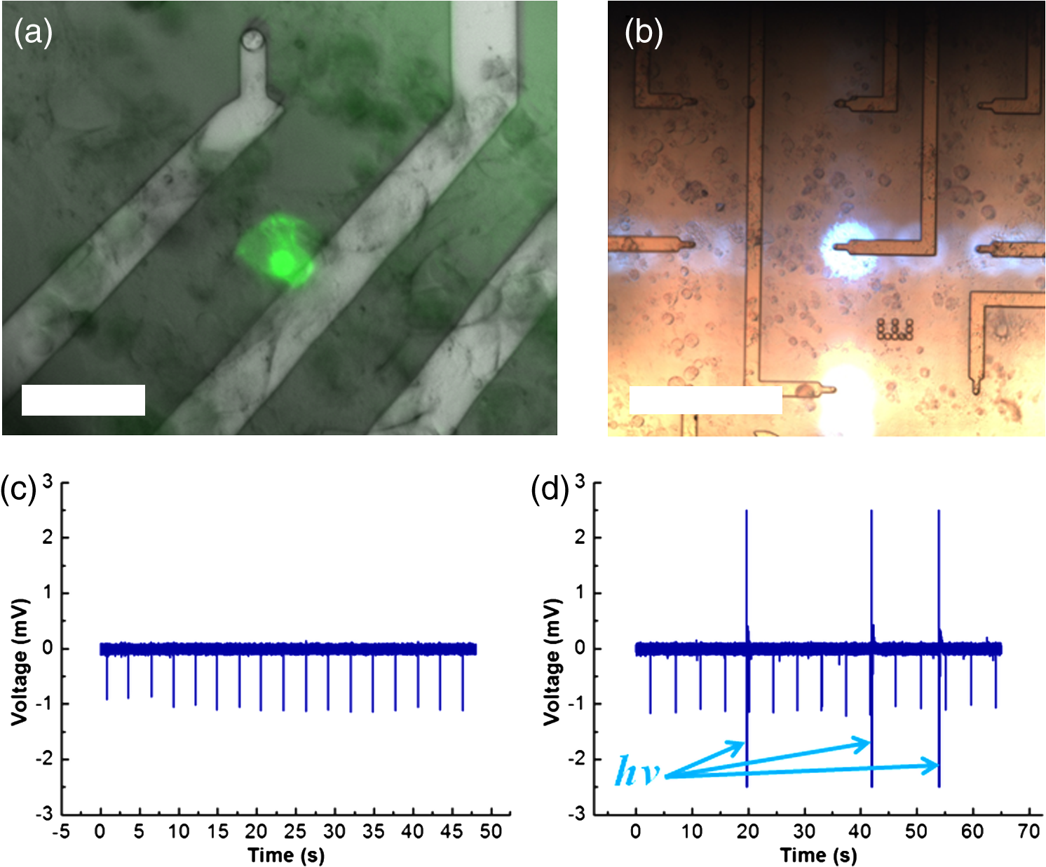 3.3.Electrical RecordingsGenerally, after having formed a tight monolayer, HL-1 cells started beating spontaneously if there were enough nutrients and, most importantly, norepinephrine in the medium. In this case, the pacemaker cell initiating the beating was located at an arbitrary position on the chip surface. Electrical activity from HL-1 cells could be readily recorded with the μLED-MEA device. Figure 3 shows signals from spontaneously beating HL-1 cells with amplitudes of up to 1 mV. As opposed to standard patch clamp recordings, the signals are inverted and partially distorted due to the recording of extracellular voltage transients via capacitive coupling at the cell-microelectrode junction. The signal-to-noise ratio of the extracellular AP recordings is somewhat lower than in previously reported experiments using nanocavity electrode arrays.33,34 This can be explained by the limited electrode-electrolyte interface that is predetermined by the small size of the electrodes necessary to avoid extensive blocking of light in the μLED-MEA device. One way of addressing this challenge is to increase the electrode-electrolyte interface without increasing the geometric electrode size by introducing a nanopatterned electrode surface.35 There have been many research efforts in this direction which effectively demonstrated improved cell-electrode coupling using various patterned electrode systems.15,36–38 Such an approach could be integrated into the future modifications of the μLED-MEA device to further improve the signal-to-noise ratio. We have tried to stimulate a transfected cell within a beating monolayer in order to hijack the pacemaking function from the randomly established pacemaker cell to a specific cell chosen by us. Different light intensities were delivered in 100 ms pulses via regulating the pixel bias voltage from 3 to 10 V [Fig. 3(b)]. These light pulses resulted in electrical artifacts sensed by the recording system [Fig. 3(d)], such as blind periods, where no recordings could be seen for about 20 to 40 ms after light stimulation. The extent of these artifacts is similar to the ones produced by on-chip electrical stimulation which, in turn, depend on the electrode impedance of the microelectrodes. Regardless of the applied μLED intensity, hijacking or disturbing the natural pacemaker function was not successful. One possible explanation for this is that the pulses were reaching the cell during the refractory period. Nevertheless, increasing pulse time to deliberately cover more than one AP period (1 s pulse time) did not change the spontaneous activity. We believe that the synchronized beating is very stable and depolarization of a single cell within the monolayer, with light intensities deliverable by the μLED-MEA chip, could not easily reverse the entire AP wave of the network. 3.4.Ca-Imaging RecordingsAccording to known intensity values, a single μLED pixel should be sufficient to depolarize ChR2 protein, as was successfully shown in previous works using external light sources.12,32 In order to demonstrate direct on-chip optical stimulation, we have performed experiments on a nonbeating “silent” culture of HL-1 cells. The cells were confluent and had started to form gap junctions without displaying spontaneous activity yet. Ca-Imaging with the dye Fura-2, sensitive to intracellular concentrations, was used to map the light stimulated activity in HL-1 cell networks. A fast acquisition mode with temporal resolution of 30.54 ms (32.74 fps) was used, thus, utilizing the fast scanning mode of the EM-CCD camera. Several different fields of 4 by 4 pixels, i.e., , situated around transfected cells, were illuminated with 500 ms long pulses with intensity of approximately . These stimulations resulted in successful depolarizations of the cells and initiation of AP-waves across the filmed area, as can be seen in Video 1. Stimulating experiments of nontransfected cells failed to produce any APs. Thus, the stimulation is, indeed, assumed to be a result of light application and not, for instance, a thermal effect. Besides, according to previous investigations, the thermal effect for μLED, with sizes below 20 μm, is basically minimized. The smaller the pixel size, the lower is the junction temperature under the same current density.39,40 To aid video-analysis of the AP-wave, the raw video was resliced so that the 2D projection incorporates one spatial dimension ( or position on the chip) along the horizontal and time along the vertical. The reformatted videos, thus, show calcium events over time at a single position in each frame and subsequent frames show neighboring positions on the chip. Figure 4 shows a snapshot from the resliced video recording in the time— projection (Video 2) and the image analysis of the video. Induced APs are clearly seen after the stimulation pulses, arriving on average after the stimulation (, error is s.d.). Although the AP-wave arrival times are quite scattered (minimum is 580 ms, maximum 1680 ms), they appear in discrete values (e.g., 1497 ms exactly two times, and 886 ms exactly two times), indicating that different individual cells across the chip were excited to artificially act as pacemakers. The stimulation field was situated outside the recording area so that the CCD camera would not be saturated and damaged by the stimulation light pulse. In principle, one could assume, that the activity of the cells would be triggered as soon as the light induced ionic currents through the channels are sufficiently large to cause depolarization of the membrane. To investigate the observed delay between stimulation and network activity, we analyzed the propagation speed of the calcium wave across the monolayer. The signal propagation lies in the range of , which is in agreement with previous measurements of similar HL-1 networks.28 However, taking into account the lateral dimensions of our system, it cannot explain delays beyond 200 ms. Thus, we attribute the delay to the relatively weak light-intensities delivered during on-chip optical stimulation. A similar effect has been observed for laser-induced light stimulation of ChR2 transfected cells. At low light intensities, delays in the electrophysiological signals, of more than 100 ms after stimulation, were recorded.28 Thus, future work for the improvement of the presented on-chip optoelectrical recording and stimulating system should be directed at increasing pixel light intensities for more efficient stimulation of single cells. Fig. 4Calcium imaging of the transfected ChR2 HL-1 cells stimulated with light using μLED-MEA chip. (a) Intensity profile over the entire frame area. (b) Intensity of the resliced image in the time—y projection. (c) Light stimulation pulses. 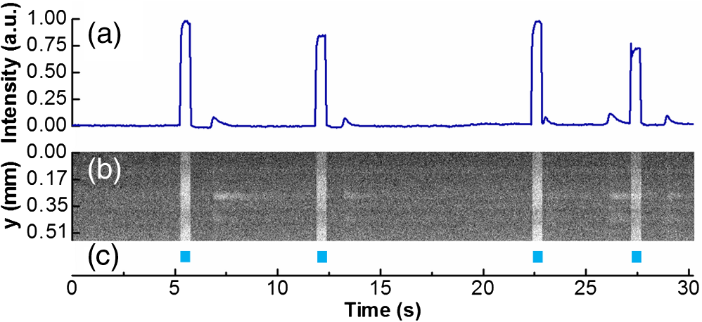 Video 1Ca-imaging of a ChR2-transfected HL-1 cell network grown on a µLED-MEA device. Repetitive cellular responses across the chip can be seen after successful stimulations of cells with illumination from fields of 4 by 4 µLED pixels, i.e. , with an intensity of approximately . The temporal resolution of the video recorded with an EM-CCD camera was 30.54 ms (32.74 fps) [URL: http://dx.doi.org/10.1117/1.JBO.18.11.111402.1].  Video 2Reslicing of the raw data from Supplementary Video 1. 2D projection of the original video incorporates one spatial dimension (-axis on the chip) along the horizontal axis and time along the vertical axis. The video shows calcium events over time at a single position in each frame and subsequent frames show neighboring positions on the chip [URL: http://dx.doi.org/10.1117/1.JBO.18.11.111402.2].  4.ConclusionsWe have demonstrated the design, fabrication, and application of an optoelectrical device capable of optical stimulation and electrical recording from light-sensitive electrogenic cells. A combined modular chip was fabricated consisting of an array of 841 addressable micropixellated InGaN light-emitting diodes coupled to a custom-made MEA with 64 microelectrodes on an ultrathin, transparent substrate. All diodes and microelectrodes could be addressed individually. Cardiomyocyte-like HL-1 cells were transfected with ChR2 and cultured on the chip. Blue light pulses delivered by the μLED-MEA chip had intensities sufficient for the activation of ChR2. Light stimulation by μLED-MEA resulted in the depolarization of cells and subsequent calcium transients. Electrical measurements from monolayers of spontaneously beating HL-1 cells using μLED-MEAs were performed to assess the recording capabilities of the chip. On-chip optical stimulation, with increasing light intensities, was not sufficient to hijack the natural pacemaker function and redirect the AP wave in the HL-1 monolayer. On the contrary, nonbeating HL-1 cells could be triggered optically on-chip to initiate APs in a repeatable manner. The triggered APs were recorded by calcium imaging. We see the potential of μLED-MEA chips for experiments with optogenetically modified cells. The device allows optical stimulation of in vitro cultures with approximately single cell resolution at arbitrary positions of the active area and electrical recordings with single cell resolution. For a variety of applications, including highly focused optical stimulation, an external microscopic projection approach will remain the method of choice. However, the combined system of the μLED-MEA, presented here, can be used in a stand-alone, lab-on-a-chip assay for experiments that are performed in standard incubators. For such investigations, the chip-based approach is more versatile and avoids the need of integrating incubation chambers into the microscopic setup. The main advantage lies in light stimulation and extracellular electrical recording capabilities without complex optics or external light sources rendering it suitable for long-term measurements. AcknowledgmentsWe thank Norbert Wolters for the development of electronics and Dieter Lomparski and Michael Jansen for software development. Additionally, we thank Francesca Santoro for the help with cell culture. This work was partially funded by the Helmholtz Young Investigators program. ReferencesK. Deisseroth,
“Optogenetics,”
Nat. Methods, 8
(1), 26
–29
(2011). http://dx.doi.org/10.1038/nmeth.f.324 1548-7091 Google Scholar
E. S. Boydenet al.,
“Millisecond-timescale, genetically targeted optical control of neural activity,”
Nat. Neurosci., 8
(9), 1263
–1268
(2005). http://dx.doi.org/10.1038/nn1525 NANEFN 1097-6256 Google Scholar
J. Y. Lin,
“A user’s guide to channelrhodopsin variants: features, limitations and future developments,”
Exp. Physiol., 96
(1), 1925
(2010). http://dx.doi.org/10.1113/expphysiol.2009.051961 EXPHEZ 0958-0670 Google Scholar
J. Y. Linet al.,
“Characterization of engineered channelrhodopsin variants with improved properties and kinetics,”
Biophys. J., 96
(5), 1803
–1814
(2009). http://dx.doi.org/10.1016/j.bpj.2008.11.034 BIOJAU 0006-3495 Google Scholar
T. Knöpfelet al.,
“Toward the second generation of optogenetic tools,”
J. Neurosci., 30
(45), 14998
–15004
(2010). http://dx.doi.org/10.1523/JNEUROSCI.4190-10.2010 JNRSDS 0270-6474 Google Scholar
A. M. Aravaniset al.,
“An optical neural interface: in vivo control of rodent motor cortex with integrated fiberoptic and optogenetic technology,”
J. Neural. Eng., 4
(3), S143
–S156
(2007). http://dx.doi.org/10.1088/1741-2560/4/3/S02 1741-2560 Google Scholar
L. Wenet al.,
“Opto-current-clamp actuation of cortical neurons using a strategically designed channelrhodopsin,”
PLoS One, 5
(9),
(2010). http://dx.doi.org/10.1371/journal.pone.0012893 1932-6203 Google Scholar
V. Gradinaruet al.,
“Optical deconstruction of Parkinsonian neural circuitry,”
Science, 324
(5925), 354
–359
(2009). http://dx.doi.org/10.1126/science.1167093 SCIEAS 0036-8075 Google Scholar
I. B. Wittenet al.,
“Cholinergic interneurons control local circuit activity and cocaine conditioning,”
Science, 330
(6011), 1677
–1681
(2010). http://dx.doi.org/10.1126/science.1193771 SCIEAS 0036-8075 Google Scholar
A. B. Arrenberget al.,
“Optogenetic control of cardiac function,”
Science, 330
(6006), 971
–974
(2010). http://dx.doi.org/10.1126/science.1195929 SCIEAS 0036-8075 Google Scholar
J. Wanget al.,
“Laser-evoked synaptic transmission in cultured hippocampal neurons expressing channelrhodopsin-2 delivered by adeno-associated virus,”
J. Neurosci. Methods, 183
(2), 165
–175
(2009). http://dx.doi.org/10.1016/j.jneumeth.2009.06.024 JNMEDT 0165-0270 Google Scholar
N. Grossmanet al.,
“Multi-site optical excitation using ChR2 and micro-LED array,”
J. Neural Eng., 7 016004
(2010). 1741-2560 Google Scholar
F. Zhanget al.,
“Multimodal fast optical interrogation of neural circuitry,”
Nature, 446
(7136), 633
–639
(2007). http://dx.doi.org/10.1038/nature05744 NATUAS 0028-0836 Google Scholar
M. ScanzianiM. Häusser,
“Electrophysiology in the age of light,”
Nature, 461
(7266), 930
–939
(2009). http://dx.doi.org/10.1038/nature08540 NATUAS 0028-0836 Google Scholar
M. E. SpiraA. Hai,
“Multi-electrode array technologies for neuroscience and cardiology,”
Nat. Nano., 8
(2), 83
–94
(2013). http://dx.doi.org/10.1038/nnano.2012.265 1748-3387 Google Scholar
A. Stettet al.,
“Biological application of microelectrode arrays in drug discovery and basic research,”
Anal. Bioanal. Chem., 377
(3), 486
–495
(2003). http://dx.doi.org/10.1007/s00216-003-2149-x ABCNBP 1618-2642 Google Scholar
W. L. C. Rutten,
“Selective electrical interfaces with the nervous system,”
Annu. Rev. Biomed. Eng., 4
(1), 407
–452
(2002). http://dx.doi.org/10.1146/annurev.bioeng.4.020702.153427 ARBEF7 1523-9829 Google Scholar
E. Ben-JacobY. Hanein,
“Carbon nanotube micro-electrodes for neuronal interfacing,”
J. Mater. Chem., 18
(43), 5181
–5186
(2008). http://dx.doi.org/10.1039/B805878B JMACEP 0959-9428 Google Scholar
Z. Gonget al.,
“Matrix-addressable micropixellated InGaN light-emitting diodes with uniform emission and increased light output,”
IEEE Trans. Electron Devices, 54
(10), 2650
–2658
(2007). http://dx.doi.org/10.1109/TED.2007.904991 IETDAI 0018-9383 Google Scholar
C. Bamannet al.,
“Spectral characteristics of the photocycle of channelrhodopsin-2 and its implication for channel function,”
J. Mol. Biol., 375
(3), 686
–694
(2008). http://dx.doi.org/10.1016/j.jmb.2007.10.072 JMOBAK 0022-2836 Google Scholar
B. K. Andrasfalvyet al.,
“Two-photon single-cell optogenetic control of neuronal activity by sculpted light,”
PNAS, 107
(26), 11981
–11986
(2010). http://dx.doi.org/10.1073/pnas.1006620107 PNASA6 0027-8424 Google Scholar
K. Nikolicet al.,
“Photocycles of channelrhodopsin-2,”
Photochem. Photobiol., 85
(1), 400
–411
(2009). http://dx.doi.org/10.1111/j.1751-1097.2008.00460.x PHCBAP 0031-8655 Google Scholar
B. McGovernet al.,
“An optogenetic neural stimulation platform for concurrent induction and recording of neural activity,”
Proc. SPIE, 7548 75484X
(2010). http://dx.doi.org/10.1117/12.842665 Google Scholar
C. R. Beltonet al.,
“New light from hybrid inorganic–organic emitters,”
J. Phys. D Appl. Phys., 41
(9), 094006
(2008). http://dx.doi.org/10.1088/0022-3727/41/9/094006 JPAPBE 0022-3727 Google Scholar
J. Dayet al.,
“Full-scale self-emissive blue and green microdisplays based on GaN micro-LED arrays,”
Proc. SPIE, 8268 82681X
(2012). http://dx.doi.org/10.1117/12.914061 Google Scholar
H. X. Zhanget al.,
“Microstripe-array InGaN light-emitting diodes with individually addressable elements,”
IEEE Photon. Technol. Lett., 18
(15), 1681
–1683
(2006). http://dx.doi.org/10.1109/LPT.2006.879926 IPTLEL 1041-1135 Google Scholar
F. Faßbenderet al.,
“Optimization of passivation layers for corrosion protection of silicon-based microelectrode arrays,”
Sensors Actuat. B Chem., 68
(1–3), 128
–133
(2000). http://dx.doi.org/10.1016/S0925-4005(00)00472-X SABCEB 0925-4005 Google Scholar
B. Hofmannet al.,
“Light induced stimulation and delay of cardiac activity,”
Lab Chip, 10
(19), 2588
–2596
(2010). http://dx.doi.org/10.1039/C003091K LCAHAM 1473-0197 Google Scholar
T. Nagaiet al.,
“A variant of yellow fluorescent protein with fast and efficient maturation for cell-biological applications,”
Nat. Biotechnol., 20
(1), 87
–90
(2002). http://dx.doi.org/10.1038/nbt0102-87 NABIF9 1087-0156 Google Scholar
W. C. Claycombet al.,
“HL-1 cells: a cardiac muscle cell line that contracts and retains phenotypic characteristics of the adult cardiomyocyte,”
PNAS, 95
(6), 2979
–2984
(1998). http://dx.doi.org/10.1038/nbt0102-87 PNASA6 0027-8424 Google Scholar
J. K. Y. Lawet al.,
“The use of microelectrode array (MEA) to study the protective effects of potassium channel openers on metabolically compromised HL-1 cardiomyocytes,”
Physiol. Meas., 30
(2), 155
–167
(2009). http://dx.doi.org/10.1088/0967-3334/30/2/004 PMEAE3 0967-3334 Google Scholar
A. Berndtet al.,
“High-efficiency channelrhodopsins for fast neuronal stimulation at low light levels,”
PNAS, 108
(18), 7595
–7600
(2011). http://dx.doi.org/10.1073/pnas.1017210108 PNASA6 0027-8424 Google Scholar
B. Hofmannet al.,
“Nanocavity electrode array for recording from electrogenic cells,”
Lab Chip, 11
(6), 1054
(2011). http://dx.doi.org/10.1039/c0lc00582g LCAHAM 1473-0197 Google Scholar
M. Schottdorfet al.,
“Frequency-dependent signal transfer at the interface between electrogenic cells and nanocavity electrodes,”
Phys. Rev. E, 85
(3), 031917
(2012). http://dx.doi.org/10.1103/PhysRevE.85.031917 PLEEE8 1063-651X Google Scholar
B. Wolfrumet al.,
“Fabrication of large-scale patterned gold-nanopillar arrays on a silicon substrate using imprinted porous alumina templates,”
Small, 2
(11), 1256
–1260
(2006). http://dx.doi.org/10.1002/smll.200600311 1613-6829 Google Scholar
D. Brüggemannet al.,
“Nanostructured gold microelectrodes for extracellular recording from electrogenic cells,”
Nanotechnology, 22
(26), 265104
(2011). http://dx.doi.org/10.1088/0957-4484/22/26/265104 NNOTER 0957-4484 Google Scholar
J.-H. Kimet al.,
“Surface-modified microelectrode array with flake nanostructure for neural recording and stimulation,”
Nanotechnology, 21
(8), 85303
(2010). http://dx.doi.org/10.1088/0957-4484/21/8/085303 NNOTER 0957-4484 Google Scholar
R. KimN. HongY. Nam,
“Gold nanograin microelectrodes for neuroelectronic interfaces,”
Biotechnol. J., 8
(2), 206
–214
(2013). http://dx.doi.org/10.1002/biot.201200219 JBITD4 0168-1656 Google Scholar
Z. Gonget al.,
“Size-dependent light output, spectral shift, and self-heating of 400 nm InGaN light-emitting diodes,”
J. Appl. Phys., 107
(1), 013103
(2010). http://dx.doi.org/10.1063/1.3276156 JAPIAU 0021-8979 Google Scholar
T. Kimet al.,
“High-efficiency, microscale GaN light-emitting diodes and their thermal properties on unusual substrates,”
Small, 8
(11), 1643
–1649
(2012). http://dx.doi.org/10.1002/smll.201200382 1613-6829 Google Scholar
|


