
|
|
1.IntroductionIn recent years, the early detection of biological agents and markers has attracted great interest among researchers in the biosensing field. Early detection sensing technologies consist of the following characteristics: portability, user-friendliness (e.g., limited sample preparation required), and multiplexing. When a biosensing technology encounters the mentioned characteristics, it acquires high impact in many applications: food safety, homeland security, environmental and industrial monitoring, and, most importantly, medical diagnostics.1–4 The last decade has witnessed a constant technical improvement of both detection methods and instrumentations. Among other technologies, surface plasmon resonance (SPR)-based optical devices have become a front-figure. SPR biosensors have been proven to be suitable systems for label-free real-time and multiplexed detection purposes.5–11 Surface plasmons are collective charge oscillations confined at the interface between two media with dielectric constants of opposite sign.12 The plasmonic modes are characterized by an electric field that exponentially decays into the two media composing the interface. This property makes the plasmonic modes extremely sensitive to refractive index changes occurring at the interface. Since the maximum sensitivity is in a region comprised within a few tenths of nanometers above the sensing surface, these devices are ideal platforms for the label-free detection of molecular monolayers.13 Moreover, the possibility of a real-time detection of the binding events is particularly interesting for measuring the affinity between molecules. Within the great family of SPR-based optical devices, different system sensing platforms have been investigated. Particular interest has been found in metallic nanoparticles supporting localized plasmonic excitations14 due to their sensitivity to the detection of small molecules. Despite their well-performing sensing capabilities, these systems have never found a true routine industrial application. On the other hand, most of the commercially available devices exploit the surface plasmon polaritons (SPPs) propagating at the interfaces of thin metallic (usually gold) films. Because of the mismatch in the wavevector of the SPP and the incident light having the same energy, momentum-coupling techniques must be used for the SPP excitation.15 The most used sensor configuration consists of a thin metallic film deposited on the top of a high refractive index prism (Kretschmann configuration).16 The light beam impinges from the prism side at an angle greater than the total internal reflection angle. The chips for prism-based SPR detection do not require nanofabrication, and the use of a reflective geometry decouples optical signals from fluidic channels.8,17–20 However prism-based optics may be expensive and delicate, in particular in the case of plasmonic imaging systems.21–23 Alternatively, the wavevector mismatch between incident light and SPP modes can be coupled by the periodical patterning of the metal surface, with the formation of an optical grating.6,24–28 In order to function as a plasmonic coupler, the grating period needs to be in the order of the involved SPP wavelength. However, SPR sensors based on grating coupling are usually configured in such a way that the incident light is passing through the analysis liquid cell, compromising the sensitivity and the stability of such sensors.26 On the other hand, the grating coupling configuration offers the possibility of tuning the resonant wavelength by scaling the grating period while keeping fixed the angle of incidence of light. In this way, the optical constraints are greatly relaxed and a normal incidence detection scheme can be used. Normal incidence detection using telecentric optics enables facilitated plasmonic imaging of the surface over a large field of view and, contemporarily, with microscopic lateral resolution. In this paper, we present an SPR imaging system based on a nanostructured gold-polymer chip. The system enables the real-time multiplexed detection of several analytes. The sensing chip consists of a two-dimensional hexagonal array of plasma polymerized poly-acrylic acid (ppAA) nanopillars embedded in an optically thick gold film deposited on a glass substrate.29–31 The sensing performance of the surfaces (sensitivity to refractive index change and to the adhesion of molecular monolayers) has been tested using standard spectroscopic techniques. Then, an imaging biosensing device tailored on the chip response has been developed in-house and called Imaging Nanoplasmonics device (iNPx). The iNPx system integrates the fluidics, the electronics, and the computing and data analysis unit resulting in a compact, stand-alone, and fully portable device. The iNPx performance has been characterized with both sensitivity measurements on refractive index changes and detection of a model biomolecular interaction (where a receptor has been immobilized on the chip surface and the ligand dispensed on the chip by the integrated microfluidics system). Finally, to assess the performance of our system in a real diagnostic application, we focused on the detection of a new molecule, the long pentraxin 3 (PTX3). PTX3 belongs to the super family of long pentraxins and is characterized by a long, unrelated N-terminal domain associated to the C-terminal pentraxin-like domain homologous to C-reactive protein and serum amyloid P component.32 PTX3 is a multifunctional molecule rapidly and locally produced by immune and stromal cells in response to primary proinflammatory molecules and bacterial components as lipopolysaccharide, capable of interacting with several proteins, including complement components, microbial moieties, and adhesion molecules.33 Translational efforts are in progress to evaluate the role of PTX3 as a possible marker and therapeutic agent in human pathologies.34 PTX3 levels increase in cardiovascular diseases, kidney pathologies, and infections (like sepsis) and represent a new prognostic marker reflecting local activation of innate immunity and inflammation, rapidly induced, and correlating with the severity of disease.34–38 Given its relevance as a new marker of human pathologies, PTX3 is an interesting candidate to do new and exciting research in medical diagnostics. After a description of the experimental methods in Sec. 2 and optical response of the chip in Sec. 3.1, we report a characterization of the sensitivity of the sensing chip. The spectral measurement of the chip response to a refractive index change allows evaluation of the detection limit (Sec. 3.2). Reflectance measurements of the chip response to the adhesion of polyelectrolyte monolayers give the field extension of the plasmonic mode above the nanostructured surface (Sec. 3.3). In Sec. 3.4, a brief description of the instrumental configuration of the plasmonic imaging device is described. Finally, a proof-of-concept diagnostic application of the system is presented in Sec. 3.5. 2.Materials and Methods2.1.Chip FabricationThe sensing surfaces consist of a hexagonal lattice of polymeric pillars embedded in an optically thick gold film deposited on a glass substrate. The fabrication process based on colloidal lithography and plasma enhanced chemical vapor deposition (PE-CVD) is described in detail elsewhere29 and can be outlined in five steps. A ppAA film is deposited on a glass substrate by PE-CVD. By the Langmuir-Blodgett technique, a self-assembled monolayer of polystyrene spheres is transferred onto the ppAA film. Reactive ion etching is then used to completely remove the ppAA from the areas not covered by the spheres (and, simultaneously, reduce the diameter of the spheres). A gold layer is then deposited on the sample using physical vapor deposition. Finally, the residual colloidal mask is removed by a sonication bath. 2.2.Chip Optical CharacterizationThe optical characterization of the sensor chip was carried out by reflectance measurements. Most of the measurements were performed using a commercial Fourier transform spectrometer (FT-66, Bruker, Karlsruhe, Germany) equipped with a home-made variable angle micro-reflectometer. In order to test the optical scheme of our biosensor setup, a prototypal device was assembled. In the prototype, a beam splitter was used to send the light of a Xenon lamp to the sample and collect the reflected beam with a compact CCD spectrometer (OceanOptics, Dunedin, Florida). Comparison measurements were carried out with both instruments. Moreover, a double beam UV-VIS-NIR spectrometer Varian Cary6i has been used for high-sensitivity detection. The spectra were acquired in the spectral range of 400 to 1250 nm with TM polarized light incident on the samples from the substrate side. The sample holder was equipped with a home-made cell allowing the solution to flow on the chip surface. A spectroscopic ellipsometer (Sopra ESG4R) was used to determine the thickness and refractive index of polyelectrolyte films used for the sensitivity tests. 2.3.Solutions for Refractive Index CalibrationNaCl, glycerol, and ethanol solutions in ultrapure water (resistivity ) were used to monitor the changes in the optical response of the chips with respect to small refractive index variations. Concentration ranges were, respectively, between 0.0004 and 2% in weight for NaCl, between 0.0004 and 3% for glycerol, and between 0.006 and 3.16% for ethanol. An Abbe refractometer (Zeiss, Jena, Germany) was used to measure the refractive index of the more concentrated solutions down to 0.25, 0.25, and 0.8% in the case of NaCl, glycerol, and ethanol, respectively. The lowest measured refractive index differs from that of ultrapure water (used as a reference). The measured refractive indexes were used to extrapolate the refractive index changes for the solutions at the lowest concentration. Refractive index variations from refractive index units (RIU) down to with respect to water have been explored. It is important to notice that the refractive indexes of the more dilute solutions are extrapolated from those measured for solutions that are already well diluted (0.25 to 3%). In this way, the nonlinearity problem arising when the extrapolation is based on the pure solute refractive index should be avoided. To evaluate the chip response to the adhesion of nanometric layers, polyelectrolyte solutions of poly(diallyldimethylammonium chloride) (PDDA, Sigma Aldrich, St. Louis, Missouri) and of poly(sodium 4-styrenesulfonate) (PSS, Sigma Aldrich) diluted at 2% in water were used. Each polyelectrolyte solution has been injected in a liquid cell by means of a peristaltic pump, alternating a rinsing step of ultrapure water. In this way, the excess material can be removed, preparing the surface for the following injection step. 2.4.Characterization of the Imaging Nanoplasmonics Device2.4.1.Sensitivity and imaging performances with a model bioreactionCalibrated glycerol solutions as the ones used for chip surface characterization in spectroscopic mode were used for the calibration of the imaging system with respect to refractive index variations. A test of the imaging performances of the device has been instead performed using the well-known FLAG, anti-FLAG peptide system as a biomarker. FLAG® peptide (aminoacid sequence: DYKDDDDK, Sigma Aldrich) was immobilized to the carboxyl functionalized chip surface via the amine residue coupled through the standard 1-Ethyl-3-(3-dimethylaminopropyl)carbodiimide/N-Hydroxysuccinimide (EDC/NHS) activation chemistry using a microarray spotter (SciFLEXArrayer, Scienion AG, Berlin, Germany). The spots were organized in a square lattice array with a pitch of 500 μm and a spot size of . Then the microarray spotting the chip was rinsed by ethanolamine (1 M) in order to passivate the unreacted carboxyl groups. Bovine serum albumin (BSA, ) was then injected in order to eventually block residual active binding sites. The microarray plated chip was then sealed to a microfluidics cell (10 μL volume) and inserted in the iNPx reader. Ab-FLAG detection experiments have been performed online using the in-house developed analysis software. Briefly, the software continuously acquires the camera frames (maximum acquisition rate 35 fps) and elaborates averaged pictures. The number of averaged frames affects both the time resolution and the noise level. The averaged picture is then processed by the software in order to evaluate the reflectance variations occurring on the chip surface. The reflectance variations are monitored in real time in the following way:
2.4.2.Biodetection of the marker for sepsis in imaging modeBiosensing imaging assay was performed on plasmonic chips by covalent immobilization of antibodies raised against PTX3 (Ab-PTX3) on self-assembled mercaptohexadodecanoic acid monolayers via EDC/NHS activated covalent binding. Selective surface functionalization and immobilization of the Ab-PTX3 was performed using microcapillary pumps consisting of seven independent microchannels. This is a simple Polydimethylsiloxane (PDMS) microfluidics device fabricated in-house, enabling the localized immobilization with controlled flow of different molecules or chemicals. All the seven channels were activated using EDC/NHS protocol. Four of the seven microchannels (from top: channels 1, 3, 5, 7) were loaded overnight with Ab-PTX3 ( in 10 mM acetate buffer, ), while three of them were loaded with acetate buffer (2, 4, 6) only and used as negative control. PTX3 was purified by immunoaffinity from the supernatant of chinese hamster ovary transfected cells. Purified recombinant PTX3 () and 1% BSA (used as blocking solution) were diluted in phosphate-buffered saline (PBS, , Invitrogen, Carlsbad, California). Rat monoclonal antibodies and rabbit polyclonal antiserum were obtained by immunizing animals with purified recombinant PTX3.39 3.Results and Discussion3.1.Analysis of the Chip Optical ResponseA complete optical characterization of the sensing surfaces has been reported in previous papers.29,30 The optical response of these surfaces can be interpreted in terms of plasmonic excitation localized inside the ppAA pillar (the main resonance is shown as a reflectance minimum at to 900 nm) and SPP propagating at the film interfaces (characterized by lower wavelengths around 550 nm). The localized modes enable the coupling between the SPPs supported by the opposite film interfaces, even if the gold film is relatively thick (). This allows detection of a refractive index change at the free surface of the chip by measuring reflectance spectra with light incident from its substrate side. Figure 1(a) shows the reflectance spectrum between 840 and 910 nm measured with TM polarized light at nearly normal incidence, when pure water (dashed line) or a solution of water with 2% NaCl (solid line) are flowing inside the liquid cell. The refractive index change induces a shift of the resonance minimum of . The chip response can be simply visualized as the ratio between the two reflectance spectra [Fig. 1(b)]. The value of such a ratio, corresponding to both positive (maxima) and negative (minima) intensity variations with respect to 1, is directly proportional to the spectral shift at each wavelength. Fig. 1(a) Detail of the chip reflectance spectra measured by TM polarized light at 5 deg incidence angle from the glass side of the sample when the flow cell is filled with ultrapure water (milliQ) (red dashed line) or with a 2% NaCl solution (black solid line). (b) Ratio of the reflectances shown in (a): R(NaCl 2% solution)/R(distilled water) (black line). The blue dash-dot line corresponds to the quantity with , uniform over the whole spectral interval. Despite the small vertical shift, the difference between maximum and minimum is the same for both curves.  The ratio can be expressed as and approximated by . Figure 1(b) shows the ratio of the reflectance curves reported in panel (a). The dash-dot curve in panel (b) represents the approximate ratio expression when a , constant over the whole considered range, is assumed. The expression linearly correlates the relative change of the reflectance with the spectral shift . Such a change is proportional to the steepness of the reflectance spectrum and reaches its maxima amplitudes at 850 nm () and 900 nm (). Nevertheless, due to the large spectral width of the plasmonic mode, these maxima are spectrally broad. Moreover, since the response in terms of positive- or negative- change is referred to the same spectral shift , the two signals can be combined and summed into a unique parameter, as shown by the arrow in Fig. 1(b). In a first approximation, the so-defined signal amplitude is insensitive to drift effects of the measured reflectance spectra. 3.2.Chip Response to Refractive Index VariationsThe chip sensitivity to small refractive index changes has been evaluated. We measured the near-normal incidence reflectance of the chip with water-ethanol, -glycerol and -NaCl, at different concentrations, flowing on the chip surface. The solutions were made using different solute molecules in order to monitor the occurrence of interaction effects with the chip surface and to disentangle them from the bare refractive index effect. The spectra were divided by the reflectance of ultrapure water and analyzed, as explained in Sec. 3.1. After preparation, solution and reference samples were left in the measurement room for 12 h in order to let the temperature stabilize. The refractive index of the reference water and of the concentrated solutions was directly measured with the Abbe refractometer [Fig. 2(a)]. Fig. 2(a) Measured refractive index change with respect to distilled water for NaCl (open circles), glycerol (filled triangles), and ethanol (filled squares) as a function of the solution concentration. (b) Chips response to NaCl (open circles), glycerol (filled triangles), and ethanol (filled squares) solutions with different concentrations. The plot displays the amplitude changes in reflectance referred to the reflectance of ultrapure water. (c) Plot in logarithmic scale of the same data as (b) for the low concentration data.  Then, reflectance measurements were performed by making pure water to flow first in the cell and then the solution at a given concentration. As a final step, the sample surface and the cell were rinsed with ultrapure water and the reflectance spectrum was measured again. After each injection step, spectra were acquired until the signal was definitely stabilized. The reflectance intensity variation was evaluated during the change from water to salt-, glycerol-, or ethanol-solution, and from the solution to water. The test was repeated several times and on different samples. The -axis error bar was fixed as the largest value-excursion for each refractive index variation. In fact, at the lowest concentrations, the main source of drift is represented by the temperature variations. The refractive index of water is proportional to the temperature variation rate of .40 A temperature fluctuation of 0.01°C affects the refractive index by the order of , i.e., on the order of magnitude of the refractive index variation corresponding to the lowest concentration of glycerol, ethanol, and NaCl. A careful reading of the data before, during, and after each measure is needed in order to discriminate the variations in the spectrum induced by the refractive index change. This problem is less important in the imaging system presented below because it is possible to optimize a reference ROI for normalizing the temperature drift. Figure 2 also shows that the signal amplitude is roughly independent of the solution used, indicating that the signal variation depends mainly on the refractive index change and not on the eventual chemical species absorbed by the nanostructured surfaces. 3.3.Chip Response to Layer AdhesionThe sensitivity in the region close to the top of the nanocavities has been measured by the sequential absorption of molecular monolayers, each of them characterized by a calibrated thickness. In this way, the direct evaluation of the plasmonic field profile above the surface has been carried out. The measurement was performed by alternately injecting on the chip surface a solution of polyelectrolyte molecules positively and negatively charged (PDDA and PSS, respectively). First, the chip was coated with a PDDA layer, which is immobilized on the surface by the negative charges of the ppAA pillars. Once the first positive-charged PDDA layer is deposited, a layer of negatively charged PSS layer is easily formed. The alternate deposition was repeated for at least 30 times. After each deposition step, the sample surface was rinsed with flowing water in order to remove residual unbounded molecules. The calibration of the thickness of polyelectrolyte layers was previously carried out by ellipsometry. Polyelectrolyte layers were deposited on a ppAA-coated, as well as on a gold-coated flat silicon surface. Ellipsometric measurements performed after each deposition step allowed for the monitoring of the polyelectrolyte film thickness and for the check of the nominal refractive index value of 1.5.41 The thicknesses of polyelectrolyte layers grown on ppAA substrate are in agreement with the nominal values during the first 10 deposition steps (1 and 3 nm for PDDA and PSS, respectively41). For the following steps, the film total thickness increases by each time. This behavior may be due to a nonuniform adhesion of the polyelectrolyte chains, which could be given by an outstretched or curled configuration, or a nonuniform density of the deposited layers. When gold is used as a substrate, the thickness measured after the first deposition step is equal to zero, indicating that PDDA does not adhere to the gold surface and that the first stable layer is made of PSS. As observed also for the ppAA substrate, in subsequent deposition steps, the thickness of the film increases after each polyelectrolyte layer deposition. The reflectance characterization of the alternate deposition of PDDA and PSS on the ppAA-gold nanoplasmonic surface is shown in Fig. 3. After the first step of PDDA deposition, the reflectance spectrum changes with respect to that measured with ultrapure water inside the flow cell, as shown in Fig. 3(a). The adhesion of the PDDA molecules to the chip determines a shift of the plasmonic resonances related to both localized and delocalized mode, which results in two sigmoidal structures centered, respectively, at 900 and at 590 nm. The 900-nm structure is attributed to the localized plasmonic modes, while the 590-nm structure is attributed to the SPP modes. After rinsing with water, the localized signal decreases, while the signal related to the SPP modes disappears. This result is in accordance with the ellipsometric calibration of the PDDA absorption on gold and ppAA flat surfaces: the PDDA is deposited only on the ppAA pillar top, where the localized plasmonic modes are mainly effective due to the distribution of the electric field. Figure 3(b) reports the signal evolution for the first four deposition steps. In the second deposition step, the PSS solution was injected into the flow cell and the signal reached a stable value after few seconds. The adhesion of PSS molecules to the sample surface induced an additional shift of the main spectral features. In the case of PSS adhesion, the amplitude of the signals related to both localized and delocalized modes was larger with respect to the amplitudes measured for the PDDA adhesion due to the higher thickness of the PSS layer with respect to the PDDA one. The subsequent water rinsing gave only a slight decrease of the observed signals: in this case, the spectral feature related to the SPP mode did not disappear since PSS molecules could also adhere to the gold portion of the chip surface. During the third deposition step, the PDDA molecules adhere to the whole sensor area because of the presence of the PSS layer. As a consequence, the water rinsing gives only a slight decrease of the signals related to both localized and delocalized modes. A quantitative evaluation of the localized plasmonic mode signal evolution during the first four steps of alternate PDDA/PSS deposition was carried out. During the first deposition of PDDA, the molecules adhere only to the top of the pillars and produce a signal increase of ; in contrast, the PSS molecules cover the whole chip surface and produce a signal increase of . Since the PSS layer has a thickness that is three times larger than that of the PDDA layer, assuming that the signal increase is linear in the first few deposition steps, we can deduce that a 1-nm-thick PSS layer produces a signal increase of . This is roughly the value obtained as a difference between the third (PDDA layer) and the second step (PSS layer). In this case, the signal measured by covering only the pillar top is one-third of the one obtained by covering the whole sample surface. Such a value appears almost one order of magnitude larger than what one might expect by considering the bare ratio of the area occupied by the pillar top to the whole sensor surface. Such a signal enhancement is due to the localization of the electric field at the top of the pillar as shown in a previous publication.31 Fig. 3Chip response to the adhesion of polyelectrolytes monolayers. (a) The spectral changes after the deposition of the first polydiallyldimethylammonium chloride layer before (solid line) and after (dashed line) the rinsing with pure water. Red bars indicate the localized mode and surface plasmon polariton (SPP) signal amplitude. (b) The evolution of the signal around 900 to 950 nm, related to the shift of the localized mode (filled squares) and the one relative to the SPP mode (open circles), during the first four steps of the deposition sequence. (c) The signal related to both the localized and SPP modes after rinsing for each step, as a function of the increasing thickness of the deposited polyelectrolytes film. 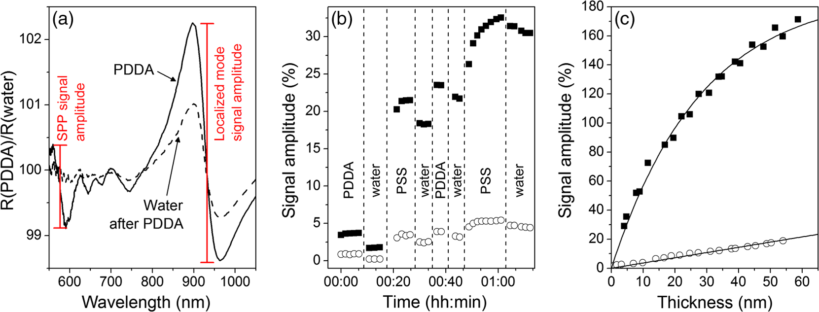 Figure 3(c) illustrates the signal amplitude recorded after the rinsing with ultrapure water for both localized and delocalized modes, displayed as a function of the polyelectrolyte layer thickness after many successive deposition steps. Since the localized mode is strongly confined inside the dielectric pillar top, its signal amplitude is plotted as a function of the layer thickness calibrated by ellipsometry on the flat ppAA surface. In contrast, since the SPP mode is mainly supported by the gold surface, the SPP mode signal amplitude is plotted as a function of the layer thickness measured on flat gold. Such a distinction affects only the first few layers. After a layer thickness of , which is obtained within the first 20 deposition steps, the signal amplitude related to the localized mode exhibits a saturation behavior, i.e., the signal increments are smaller the further the distance from the chip surface. On the contrary, the signal related to the SPP mode maintains an almost linear behavior. Since the signal amplitude is considered proportional to the effective electric field intensity at the exposed surface, the saturation behavior allows us to determine the penetration depth (i.e., the decay with the distance) of the electric field in proximity of the chip surface. The experimental data of the localized mode can be fitted by the equation , where is a constant related to the saturation value, is the thickness of the whole polyelectrolyte layer that is progressively deposited, and is the electric field penetration depth. The best fit gives a value for the penetration depth of . This is in agreement with the value reported in the literature for localized plasmonic modes, whose penetration depth is of the order of tens of nanometers. In contrast, the curve related to the delocalized mode does not show any tendency of saturation, indicating a larger penetration value with respect to the localized mode. As a matter of fact, the values reported in the literature for the penetration depth of delocalized modes are in the order of hundreds of nanometers. The simultaneous presence of localized and delocalized plasmonic resonances makes the investigated surface sensitive to two different length scales. This is particularly interesting for the possibility of detecting small molecules. 3.4.iNPx: Biosensing, Imaging, and Time Resolution CapabilitiesAs seen in the previous section, a refractive index increase occurring within the first tenth of nanometers close to the surface top results in a red shift of the main reflectance minimum. Reflectance is particularly sensitive to the refractive index change at the top of the nanocavities, as demonstrated by the PDDA/PSS absorption experiment. The refractive index change occurring on the surface of the chip is monitored by a surface light detector (usually a CMOS camera). If the surface is illuminated by a light-emitting diode (LED) source characterized by a smaller (larger) wavelength than the resonance, the CMOS camera will detect an increase (decrease) of the intensity of the reflected light. The increase (decrease) of the intensity of the reflected light is proportional to the relative variation of the refractive index at the surface. The image of the refractive index variations on the chip surface is transferred to the camera as reflectance variations by an optical imaging coupling system. The system is thus a plasmonic microscope based on nanostructured surfaces. This plasmonic-microscopy technology is called Imaging Nanoplasmonics™ (the trademark has been deposited by Plasmore S.r.l., Ranco (VA), Italy). The iNPx device consists of a stand-alone, portable, multiplexing, label-free imaging system with integrated optics, fluidics, electronics, and computing [see Fig. 4(a)]. The instrument weighs 6 kg and has the dimensions of a laptop computer. The microfluidic setup consists of a dual-automatic syringe system, for continuous buffer dispensing at a flow variable between 5 and , connected to a disposable microfluidic cell sealed to the nanoplasmonic chip. Injection of the sample liquid is done by loading a fixed volume loop connected to a 6-port injection automatic valve. The volume of the cell is 10 μl, while the dead volume between the loop and the liquid cell is . Images of the sample surface are acquired and analyzed in real time using an in-house program that enables contemporary acquisition of up to 10,000 sensorgrams of the corresponding ROIs. The fast acquisition time of the camera (35 fps) enables one to average a large number of frames ensuring, at the same time, a good signal-to-noise ratio while maintaining the necessary time resolution to monitor molecular association and dissociation events on the surface. The optimal compromise between time resolution and signal-to-noise ratio can be controlled by the instrument software. The imaging capability of the system also enables one to make the optimal self-referencing of the signal in the ROIs in order to compensate and correct temperature, flow, illumination, or electronics drifts. This is a further extension of the referencing procedure described in Sec. 3.1. The sensitivity of the device to the refractive index changes has been measured by using glycerol solutions. A calibration curve of the instrument is shown in Fig. 4(b). The instrument is able to detect a signal down to 4 RU (). Fig. 4(a) The Imaging Nanoplasmonics instrument used in the present work. The prepatterned plasmonic chip is plugged into the integrated microfluidic system using the slot on the side of the instrument. (b) Calibration curve with glycerol solutions for the Imaging Nanoplasmonics instrument.  The experimental steps of the Ab-FLAG binding and regeneration cycle (table in Fig. 5) were monitored with proprietary software and enabled the real-time acquisition and visualization of selected ROIs. In particular, the sensorgrams of 12 ROIs, 11 FLAG functionalized spots, and 1 in reference region (Fig. 5) show a stable baseline and RMS noise. Once the Ab-FLAG is injected by the automatic injection valve, the reflectance increases proportionally to the amount of molecules immobilized on the different ROIs. The signal amplitude saturates 100 s after the injection. The response is homogenous across the field of view, and the average value of the reflectance change measured in all the FLAG functionalized spots is 3.81% with a standard deviation of 0.17%. The FLAG-Ab-FLAG binding was successfully broken with 10 mM NaOH, resulting in a complete regeneration of the surface. Decreasing concentrations of Anti-FLAG were successively injected (not shown), resulting in a calibration curve. The value of the for the FLAG-Ab-FLAG interaction extrapolated from the calibration curve is 0.02 μM, which is in accordance with the value found in the literature.42 Fig. 5The sensorgrams for the Ab-FLAG detection from 11 ROIi corresponding to FLAG spots and 1 ROI corresponding to the negative control (orange curve) are shown. The corresponding acquired pictures for the three phases are reported above the plot in order to show the imaging capability. The detailed resolution of one spot is shown in the right side. 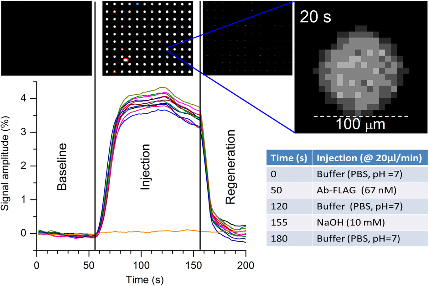 With a ½-in., camera, the lateral resolution (or the single pixel dimension) achievable with the iNPx system (zoomed picture of one FLAG functionalized spot) is 6.25 μm. Since the current field of view is of , the maximum theoretical multiplexing capability results seems to be of individual spots. Such a multiplexing capacity can only be achieved using microarrays produced with digital micromirror device–assisted synthesis that reach 10 μm resolution. 3.5.Proof-of-Concept of Diagnostic ApplicationAccording to the procedure described in Sec. 2.4, Ab-PTX3 selective immobilization has been provided inside four of the seven channels of the microfluidics device. The bright field optical image of the device is reported in Fig. 6(a). Then, the chip was mounted in the liquid cell and scanned with the iNPx instrument. The plasmonic image of the surface in air [Fig. 6(b)] gives the index contrast between air () and the PDMS () gasket of the liquid cell in contact with the surface. The PBS buffer was then continuously dispensed to the liquid cell by the microfluidic system at a constant rate of . After the acquisition of the baseline, the BSA at 1% (percentage in volume) was injected into the cell as a blocking agent for unreacted chemical groups on the surface. The difference image between the frame at and the reference picture at shows a strong reflectance contrast between the different regions of the surface [Fig. 6(c)]. In particular, the negative control channels show a higher reflectance and result brighter in the image compared to the Ab-PTX3 functionalized channels [Fig. 6(c)]. Fig. 6(a) Optical picture of the microfluidic device mounted on the plasmonic chip for surface biological patterning. (b) Plasmonic image of the patterned chip inserted in the liquid cell of the fluidic system of the iNPx instrument. (c) Ratio of the plasmonic images taken at and for the blocking step. The functionalized and control channels are put into evidence.  After having recorded a new reference image, and restarted the acquisition, PTX3 at was injected in the cell for 10 min. As shown in the sensorgram reported in Fig. 7(a), channels with the Ab-PTX3 immobilized exhibit a slightly higher reflectance with respect to the negative control channels. This indicates a specific recognition of the antigen by the immobilized antibody. Nevertheless, a small nonspecific binding of molecules can be seen in the negative control channel too. The surface is then rinsed by the reference buffer, which removes the unbound/not-specifically immobilized PTX3 molecules on the reference channels. On the other hand, the PTX3 molecules immobilized by the Ab-PTX3 were stable on the surface, showing a high affinity with the antibody. Fig. 7(a) Typical sensorgrams for one of the Ab-PTX3 functionalized channels (black curve) and a negative control channel (red curve). (b) Reflectance variation measured after the rinsing of the chip with buffer. The signal is stable and homogenous inside the channels functionalized by the Ab-PTX3, while the reference channels go back to zero level as shown in the sensorgram.  We can conclude that the stable signal (after rinsing) related to the PTX3 recognition inside the Ab-PTX3 immobilized channels corresponds to a 0.1% variation of reflectance, while the signal in the negative control channel is considerably smaller. In order to amplify the specific immobilization-related signal in the Ab-PTX3 functionalized channels, and confirm the specificity of the detection, a secondary antibody was injected onto the chip at a concentration of . Figure 7(a) reports also the evolution of the signal after this further step. When the secondary antibody is injected and after the rising with the buffer, the reflectance change with respect to the baseline rises to , confirming the specificity of the PTX3 recognition. The difference image in Fig. 7(b) corresponds to the difference between the image at and the image at . It is possible to notice how the specific recognition of the Ab-PTX3 inside the Ab-PTX3 functionalized channels results in a higher reflectance and how the signal is homogenous in the four Ab-PTX3 functionalized channels. 4.ConclusionsIn this paper, we characterized a new label-free multiplexed biosensing instrument based on the special optical properties of a nanostructured chip consisting of a lattice of polymeric pillars embedded in a gold matrix and an integrated imaging device. The characterization of the biosensing performance of the instrumentation has been carried out with the following steps:
AcknowledgmentsThe financial support of Regione Lombardia through the project SEPSIS and of the European Commission (FP7-HEALTH-2011-ADITEC-280873 and FP7-HEALTH-2011-HiPAD-278831) is gratefully acknowledged. The authors are also indebted with Mr. Giovanni Maselli of JRC-Ispra for his technical support and to Dr. Radoslaw Bombera for the support in the FLAG experiments. ReferencesA. QureshiY. GurbuzJ. H. Niazi,
“Biosensors for cardiac biomarkers detection: a review,”
Sens. Actuators B, 171–172 62
–76
(2012). http://dx.doi.org/10.1016/j.snb.2012.05.077 SABCEB 0925-4005 Google Scholar
A. P. F. Turner,
“Biosensors: sense and sensibility,”
Chem. Soc. Rev., 42
(8), 3184
–3196
(2013). http://dx.doi.org/10.1039/c3cs35528d CSRVBR 0306-0012 Google Scholar
K. R. Rogers,
“Recent advances in biosensor techniques for environmental monitoring,”
Anal. Chim. Acta, 568
(1–2), 222
–231
(2006). http://dx.doi.org/10.1016/j.aca.2005.12.067 ACACAM 0003-2670 Google Scholar
B. Van Dorstet al.,
“Recent advances in recognition elements of food and environmental biosensors: a review,”
Biosens. Bioelectron., 26
(4), 1178
–1194
(2010). http://dx.doi.org/10.1016/j.bios.2010.07.033 BBIOE4 0956-5663 Google Scholar
J. N. Ankeret al.,
“Biosensing with plasmonic nanosensors,”
Nat. Mater., 7
(6), 442
–453
(2008). http://dx.doi.org/10.1038/nmat2162 NMAACR 1476-1122 Google Scholar
A. G. Broloet al.,
“Surface plasmon sensor based on the enhanced light transmission through arrays of nanoholes in gold films,”
Langmuir, 20
(12), 4813
–4815
(2004). http://dx.doi.org/10.1021/la0493621 LANGD5 0743-7463 Google Scholar
X. D. HoaA. G. KirkM. Tabrizian,
“Towards integrated and sensitive surface plasmon resonance biosensors: a review of recent progress,”
Biosens. Bioelectron., 23
(2), 151
–160
(2007). http://dx.doi.org/10.1016/j.bios.2007.07.001 BBIOE4 0956-5663 Google Scholar
J. Homola,
“Surface plasmon resonance sensors for detection of chemical and biological species,”
Chem. Rev., 108
(2), 462
–493
(2008). http://dx.doi.org/10.1021/cr068107d CHREAY 0009-2665 Google Scholar
Y. LiX. LiuZ. Lin,
“Recent developments and applications of surface plasmon resonance biosensors for the detection of mycotoxins in foodstuffs,”
Food Chem., 132
(3), 1549
–1554
(2012). http://dx.doi.org/10.1016/j.foodchem.2011.10.109 FOCHDJ 0308-8146 Google Scholar
H. ŠípováJ. Homola,
“Surface plasmon resonance sensing of nucleic acids: a review,”
Anal. Chim. Acta, 773 9
–23
(2013). http://dx.doi.org/10.1016/j.aca.2012.12.040 ACACAM 0003-2670 Google Scholar
C. Situet al.,
“Advances in surface plasmon resonance biosensor technology towards high-throughput, food-safety analysis,”
Trends Analyt. Chem., 29
(11), 1305
–1315
(2010). http://dx.doi.org/10.1016/j.trac.2010.09.003 TTAEDJ 0165-9936 Google Scholar
H. Rather, Surface Plasmons on Smooth and Rough Surfaces and on Gratings, 111 Springer-Verlag, Berlin/Heidelberg
(1988). Google Scholar
X. Fanet al.,
“Sensitive optical biosensors for unlabeled targets: a review,”
Anal. Chim. Acta, 620
(1–2), 8
–26
(2008). http://dx.doi.org/10.1016/j.aca.2008.05.022 ACACAM 0003-2670 Google Scholar
K. A. WilletsR. P. Van Duyne,
“Localized surface plasmon resonance spectroscopy and sensing,”
Annu. Rev. Phys. Chem., 58 267
–297
(2007). http://dx.doi.org/10.1146/annurev.physchem.58.032806.104607 ARPLAP 0066-426X Google Scholar
W. L. Barnes,
“Surface plasmon-polariton length scales: a route to sub-wavelength optics,”
J. Opt. A: Pure Appl. Opt., 8
(4), S87
–S93
(2006). http://dx.doi.org/10.1088/1464-4258/8/4/S06 JOAOF8 1464-4258 Google Scholar
E. KretschmannH. Raether,
“Radiative decay of non radiative plasmons excited by light,”
Z. Naturforsch., 23A 2135
–2136
(1968). ZNTFA2 0372-9516 Google Scholar
M. PiliarikH. VaisocherováJ. Homola,
“A new surface plasmon resonance sensor for high-throughput screening applications,”
Biosens. Bioelectron., 20
(10), 2104
–2110
(2005). http://dx.doi.org/10.1016/j.bios.2004.09.025 BBIOE4 0956-5663 Google Scholar
M. Piliariket al.,
“High-resolution biosensor based on localized surface plasmons,”
Opt. Express, 20
(1), 672
–680
(2012). http://dx.doi.org/10.1364/OE.20.000672 OPEXFF 1094-4087 Google Scholar
Y. B. Shinet al.,
“A new palm-sized surface plasmon resonance (SPR) biosensor based on modulation of a light source by a rotating mirror,”
Sens. Actuators B Chem., 150
(1), 1
–6
(2010). http://dx.doi.org/10.1016/j.snb.2010.08.006 SABCEB 0925-4005 Google Scholar
E. A. SmithR. M. Corn,
“Surface plasmon resonance imaging as a tool to monitor biomolecular interactions in an array based format,”
Appl. Spectrosc., 57
(11), 320A
–332A
(2003). http://dx.doi.org/10.1366/000370203322554446 APSPA4 0003-7028 Google Scholar
C. T. CampbellG. Kim,
“SPR microscopy and its applications to high-throughput analyses of biomolecular binding events and their kinetics,”
Biomaterials, 28
(15), 2380
–2392
(2007). http://dx.doi.org/10.1016/j.biomaterials.2007.01.047 BIMADU 0142-9612 Google Scholar
E. OuelletL. LundE. T. Lagally,
“Multiplexed surface plasmon resonance imaging for protein biomarker analysis,”
Methods Mol. Biol., 949 473
–490
(2013). http://dx.doi.org/10.1007/978-1-62703-134-9 1064-3745 Google Scholar
S. Scaranoet al.,
“Surface plasmon resonance imaging for affinity-based biosensors,”
Biosens. Bioelectron., 25
(5), 957
–966
(2010). http://dx.doi.org/10.1016/j.bios.2009.08.039 BBIOE4 0956-5663 Google Scholar
A. De Leebeecket al.,
“On-chip surface-based detection with nanohole arrays,”
Anal. Chem., 79
(11), 4094
–4100
(2007). http://dx.doi.org/10.1021/ac070001a ANCHAM 0003-2700 Google Scholar
H. Imet al.,
“Nanohole-based surface plasmon resonance instruments with improved spectral resolution quantify a broad range of antibody-ligand binding kinetics,”
Anal. Chem., 84
(4), 1941
–1947
(2012). http://dx.doi.org/10.1021/ac300070t ANCHAM 0003-2700 Google Scholar
N. C. Lindquistet al.,
“Ultrasmooth metallic films with buried nanostructures for backside reflection-mode plasmonic biosensing,”
Ann. Phys. (Berlin), 524
(11), 687
–696
(2012). http://dx.doi.org/10.1002/andp.201200144 ANPYA2 0003-3804 Google Scholar
J. Martinez-Perdigueroet al.,
“Enhanced transmission through gold nanohole arrays fabricated by thermal nanoimprint lithography for surface plasmon based biosensors,”
Procedia Eng., 47 805
–808
(2012). http://dx.doi.org/10.1016/j.proeng.2012.09.269 Google Scholar
J. P. Monteiroet al.,
“Effect of periodicity on the performance of surface plasmon resonance sensors based on subwavelength nanohole arrays,”
Sens. Actuators B Chem., 178 366
–370
(2013). http://dx.doi.org/10.1016/j.snb.2012.12.090 SABCEB 0925-4005 Google Scholar
S. Giudicattiet al.,
“Plasmonic resonances in nanostructured gold/polymer surfaces by colloidal lithography,”
Phys. Status Solidi A, 207
(4), 935
–942
(2010). http://dx.doi.org/10.1002/pssa.v207:4 PSSABA 0031-8965 Google Scholar
S. Giudicattiet al.,
“Interaction among plasmonic resonances in a gold film embedding a two-dimensional array of polymeric nanopillars,”
J. Opt. Soc. Am. B, 29
(7), 1641
–1647
(2012). http://dx.doi.org/10.1364/JOSAB.29.001641 JOBPDE 0740-3224 Google Scholar
S. GiudicattiF. MarabelliP. Pellacani,
“Field enhancement by shaping nanocavities in a gold film,”
Plasmonics, 8
(2), 975
–981
(2013). http://dx.doi.org/10.1007/s11468-013-9499-9 1557-1955 Google Scholar
C. Garlandaet al.,
“Pentraxins at the crossroads between innate immunity, inflammation, matrix deposition, and female fertility,”
Annu. Rev. Immunol., 23 337
–366
(2005). http://dx.doi.org/10.1146/annurev.immunol.23.021704.115756 ARIMDU 0732-0582 Google Scholar
A. Inforzatoet al.,
“PTX3 as a paradigm for the interaction of pentraxins with the complement system,”
Semin. Immunol., 25
(1), 79
–85
(2013). http://dx.doi.org/10.1016/j.smim.2013.05.002 SEIME2 1044-5323 Google Scholar
A. Mantovaniet al.,
“Pentraxins in innate immunity: from C-reactive protein to the long pentraxin PTX3,”
J. Clin. Immunol., 28
(1), 1
–13
(2008). http://dx.doi.org/10.1007/s10875-007-9126-7 JCIMDO 0271-9142 Google Scholar
N. S. Jennyet al.,
“Associations of pentraxin 3 with cardiovascular disease and all-cause death,”
Arterioscler. Thromb. Vasc. Biol., 29 594
–599
(2009). http://dx.doi.org/10.1161/ATVBAHA.108.178947 ATVBFA 1079-5642 Google Scholar
R. Latiniet al.,
“Prognostic significance of the long pentraxin PTX3 in acute myocardial infarction,”
Circulation, 110
(16), 2349
–2354
(2004). http://dx.doi.org/10.1161/01.CIR.0000145167.30987.2E CIRCAZ 0009-7322 Google Scholar
R. Latiniet al.,
“Pentraxin-3 in chronic heart failure: the CORONA and GISSI-HF trials,”
Eur. J. Heart Fail., 14
(9), 992
–999
(2012). http://dx.doi.org/10.1093/eurjhf/hfs092 EJHFFS 1388-9842 Google Scholar
B. Muelleret al.,
“Circulating levels of the long pentraxin PTX3 correlate with severity of infection in critically ill patients,”
Crit. Care Med., 29
(7), 1404
–1407
(2001). http://dx.doi.org/10.1097/00003246-200107000-00017 CCMDC7 0090-3493 Google Scholar
L. Debanet al.,
“Regulation of leukocyte recruitment by the long pentraxin PTX3,”
Nat. Immunol., 11
(4), 328
–334
(2010). http://dx.doi.org/10.1038/ni.1854 NRIABX Google Scholar
I. ThormählenJ. StraubU. Grigull,
“Refractive index of water and its dependence on wavelength, temperature, and density,”
J. Phys. Chem. Ref. Data, 14 933
–945
(1985). http://dx.doi.org/10.1063/1.555743 JPCRBU 0047-2689 Google Scholar
M. A. Otteet al.,
“Identification of the optimal spectral region for plasmonic and nanoplasmonic sensing,”
ACS Nano, 4
(1), 349
–357
(2010). http://dx.doi.org/10.1021/nn901024e 1936-0851 Google Scholar
A. EinhauerA. Jungbauer,
“Affinity of the monoclonal antibody M1 directed against the FLAG peptide,”
J. Chromatogr. A, 921
(1), 25
–30
(2001). http://dx.doi.org/10.1016/S0021-9673(01)00831-7 JCRAEY 0021-9673 Google Scholar
BiographyBarbara Bottazzi got her doctoral degree in biological sciences in 1980 from the University of Pavia, Italy, and her PhD in pharmacological research in 1983 from Mario Negri Institute, Milan, Italy. She is mainly involved in the characterization of the long pentraxin PTX3, in particular, on the binding properties, with mapping of the domains involved in the recognition of the different ligands, and the molecular identification of the receptor for PTX3 on myeloid cells. Lucia Fornasari received her PhD degree in physics from the University of Milan in 2010. From 2011 to 2013, she was a postdoctoral fellow at the University of Pavia, in the group of Professor Franco Marabelli. She worked on a label-free biosensor based on surface plasmon resonance. Currently, she is involved in a project for the development of a detection system to monitor the bacteriological quality of drinking water. Ana Frangolho graduated from the University of Coimbra, Portugal, in chemistry in 2006. After collaborating in different projects related to protein activity, folding, and stability, with research teams from the Universities of Coimbra and Lisbon, and from the JRC in Italy, she joined Plasmore SRL in 2010 to work on nanobiointerfaces development. Currently, she is seconded to Rikilt, the Netherlands, to work in immunoassay development for biosensing. Silvia Giudicatti received her PhD in physics from the University of Pavia, Italy, in 2012. Her research activity dealt with the optical characterization and modeling of plasmonic nanostructures for biosensing applications. She is currently a postdoctoral researcher at the Institute for Integrative Nanosciences at IFW Dresden, Germany. Her work concerns the design and fabrication of titania microstructures for photonics applications. Alberto Mantovani is a professor of pathology at the University of Milan and scientific director of the Istituto Clinico Humanitas. He has contributed to the advancement of knowledge in the field of immunology, formulating new paradigms and identifying new molecules and functions. As of spring 2013, he has had over 46,400 citations and has an H-index of 119 (Scopus). Franco Marabelli received his PhD from the Swiss Federal Institute of Technology (ETH) Zurich in 1989. He is a full professor at the University of Pavia. He is responsible of the Optical Spectroscopy Laboratory at the Physics Department. His main interest is the optical spectroscopy of solid-state materials, and he has been involved in researches on heavy fermions, silicides, fullerenes, and SiGe structures. The recent topics of interest are photonic and plasmonic crystals and the optical response in semiconducting polymers. Gerardo Marchesini is a bioanalytical scientist and co-inventor of iNPx-biosensor technology. He graduated with a degree in neuroscience from the Biology School (Universidad Nacional de Cordoba), holds a PhD in bio-analytical chemistry (VU Amsterdam), and an MBA (healthcare major) from IE Business School. He is a postdoctoral fellow in analytical chemistry and nanobiotechnology in Rikilt Institute, The Netherlands, and Joint Research Center, Italy, respectively, and is currently leading the scientific and business development efforts of Plasmore. Paola Pellacani received her master degree in biomedical engineering in 2008 from Politecnico di Milano. Since 2011, she is attending the PhD School in Advanced Materials and Nanotechnology at the Universidad Autonoma de Madrid. Her research interests include nanotechnology and material science. From 2010, she works at Plasmore on development of nanostructured plasmonic sensors, focusing on biological application. She is actually involved in production and surface characterization of large-area micro- and nanostructured substrates. Rita Therisod received her master’s degree in physics in 2013 from the University of Pavia with an experimental work regarding the characterization of the optical response of nanostructured plasmonic surface in presence of refractive index change. Andrea Valsesia has a PhD in nanofabrication for bio-application from the University of Pavia, Department of Physics. He spent seven years at the Joint Research Centre-European Commission developing nanofabrication technologies for biosensing applications, publishing more than 50 papers in international peer-reviewed journals. In 2009, he founded Plasmore SRL, a spin-off company of the JRC and the University of Pavia, which develops and commercializes biosensors based on the Imaging Nanoplasmonics technology. |


