
|
|
1.IntroductionMicro- and nano-fabricated nanopores have great potential in a structural biosensor for DNA, DNA-bound proteins, and proteins by giving precise structural and pattern control of shapes1–5 and in molecular separations.5–8 Many limitations can be overcome by using a class of ultrathin membranes. It makes it possible to fabricate nanosieves having a thickness on the order of or even smaller than the diameter of the nanohole.8,9 However, membrane fragility and complex fabrication have prevented the use of ultrathin membranes for molecular separations.9–11 Furthermore, it is difficult to control the holes in nanoscale dimensions precisely and uniformly for massive production. Usually, the nanopore-based membrane nanosieves had been fabricated using silicon, silicon oxide, aluminum oxide, low-stress silicon nitride (SiN), or graphene materials1–15 for controlling the precise and reliable size control of nanopores. However, membrane nanoholes are mainly fabricated in a suspended stress-reduced silicon nitride (SiN) membrane for several reasons. Well-prepared SiN membranes can be endurable after standard micromachining processes like chemical etching (KOH, HF etc.) and have thermal stability and chemical inertness. Until now, direct electron beam writing followed by reactive ion etching (RIE), focused ion beam (FIB) etching, or focused electron beam of a transmission electron microscope (TEM) has been used to form holes in the SiN membrane.4,5,9,14,15 In case of direct hole drilling by FIB, TEM, or E-beam direct writing, their applications for many holes are very difficult, expensive, and time consuming. Since the suspended SiN membranes have to endure handling process during the fabrication and applications, its thickness and material properties should be made sufficient. Thus, the relatively thick membrane is easy to form the small pores because of the difficulty of etching pores with high aspect ratios. Above all, mass-production micro-fabrication method of the nanopores with a reduced size of about 20 to 40 nm in diameter3,5,7 on the nanosieves simultaneously and uniformly is very essential for practical nanobio immunosensing field applications. Even though there are few reports on the size control of nanopores of the membrane nanosieves,16–18 there have been no reports on the mass-production method of the precise size reduction of nanopores for massive production of nanobio-based sensings and imagings. Therefore, we here propose a mass-producible nano-fabrication method to control or reduce pore size of nanopores for membrane nanosieve combining a nanoimprinting method and the low stress-reduced silicon nitride membrane. This method is utilizing a phenomenon that there is the natural and thermal reflow of the resist after the nanoimprinting of the master mold, and it is usually widening the imprinted pattern size.19–22 The fillet-shaped resist in the side part of resist patterns caused by thermal reflow of the resist gives the narrowing of the indented patterns. When it is utilized for the etch mask for carrying out the asymmetric RIE process, we get the quite size-reduced nanopores on the membrane. In this method, nanoimprinting-based patterning using 50-nm diameter patterned master mold could be transferred to the nanoholes with nearly 30-nm dimensions in diameter, and uniform nanoholes in array as small as about 30 nm were acquired. We expect that this technology would offer a simple but very productive way for mass fabrication of the nanopores on membranes for nanobio sensing as well as sample separations in the point-of-care application field. Here, we propose a fabrication protocol to control or reduce pore size of nanopores using the nanoimprinting method in the middle of producing membrane nanosieves. 2.ExperimentalThe process schematics for design and fabrication of the nanopores on the SiN membrane are shown in Fig. 1. As for an imprinting substrate, a layer of 50-nm thick low pressure chemical vapor deposition silicon nitride (SiN) is deposited on both sides of a 6 in silicon substrate at 800°C with a trichlorosilane:ammonia () gas flow ratio of to get low stress condition. Windows on the backside of the Si substrates are opened using RIE. Fig. 1Sequential diagrams of the fabrication process: (1) silicon master mold fabrication with the electron beam lithographic and patterns-etching processes (with 50 or 100 nm in diameter), (2) surface modification of the master mold with a self-assembled monolayer of trichlorododecylsilane and e-beam resist (ER) coating on SiN surface, (3) contact printing at 180°C and 40 bar on the ER-coated SiN surface, (4) thermal reflow of ER after contact printing and etching the SiN membrane to form the nanopores, (5) the silicon substrate backside bulk etching to the silicon nitride membrane, and (6) cleaning residue of the micro-fabricated devices.  As for patterning of silicon master mold, a layer of 100-nm thick high resolution e-beam resist (ER, ZEP520A) was coated onto the diced silicon wafers in a certain dilution state of 1 to 2 with anisole and 3000 rpm. The substrates were baked at 180°C for 300 s after spin coating. Electron-beam patterning was performed using an electron beam lithography system (ELS)-7000 lithography system from ELIONIX (Tokyo, Japan). The ER was developed for 120 s using a mixed solution of isopropyl alcohol and ZeD-N50 developer. Thus, we obtained the nano molds with a square of and a square of with a height of 100 nm, respectively. The pattern spacing of master mold is designed to be 100 to 300 nm. The ELS-7000 was operated at 100 kV accelerating voltage with a 0.5 nA beam current, and a beam step of 2.5 nm. As the first step for the nanoimprinting process, the monolayer of releasing material trichlorododecylsilane () was formed on the nanostamp surface by self-assembly in the solution phase. A layer of 100-nm thick high resolution MR-I 8010 polymer (Micro Resist Technology, Berlin, Germany) was coated onto the diced silicon wafers in a state of 2500 rpm and 30 s to be a thickness of 130 nm. The substrates were baked at 120°C for 120 s after spin coating. Imprinting is done by applying a pressure of 40 bar in the main chamber, combined with pumping of the main chamber to vacuum. During imprinting, the resin becomes a thin layer by squeezing out any extra resin. Then, the copper plate is heated and the polymerization of monomer resin is initiated. After reaching the setting temperature of 180°C at the stamp surface, a stack of stamp and substrate is held for 30 min before heating is turned off. The imprinting pressure was maintained until the substrate temperature reached 120°C. An array of nanopore holes is etched into the silicon nitride layer by using ER as a masking layer on the front side of the wafer using anisotropic RIE at 55°C with an gas flow ratio of to achieve a high aspect ratio. The sheath bias voltage of accelerates positive ions and gives the bombardment of the wafers by the resulting energetic ions.23 Finally, the dices are oxygen plasma-treated to remove the resist with a power 500 mW, and gas flow of 100 standard cubic centimeters per minute (sccm) for 30 min. Then, the silicon wafers are diced to the to include four membrane sites and then bulk-etched in potassium hydroxide (KOH) at 85°C with etch rates of until no silicon is left and the membrane is freed. The key point of the method is the micro-fabrication of a nano-sized holes array on the ultrathin SiN membranes using the phenomenon of the reflow of ER material after the contact nanoimprinting. Using the fabrication process noted above, a membrane with an area of has been made. The membrane filters are perforated with several hundreds of circular holes (25–35 nm diameter). An average minimal diameter of the nanohole array is 29.8 nm with a standard deviation of 4.3 nm. The opening factor of the filters is about 6%. The opening factor increases as the holes’ size increases. It is known that a high opening factor is necessary to get a low pressure drop and high flow rate in the nanopores. So, there is a trade-off between the size of holes and the opening factor. Among the holes’ shapes, the circular geometry has been chosen due to the smallest stress concentration in the membrane. In order to fabricate the nanohole array by using the silicon master, it will take approximately a half day to fabricate the nanohole array. In case of starting the experiment with the bulk-micromachined silicon substrate, the fabrication time can be reduced to within 3 h. 3.Results and DiscussionConsidering that the nanopores will be used for nanobio sensing, they should be strong enough to endure any aerodynamic and fluid dynamic loads. The strength of the nanopores is investigated with flat silicon nitride membranes without perforating. A pressure air flow will be applied through the membranes without perforating. By applying the flow until the membrane breaks out, the burst pressure is determined as the differential pressure at burst. The membrane of is calculated to burst at about 2 psi. Figure 2 shows scanning electron microscope (SEM) photographs of a micro-fabricated membrane before (a, b) and the thickness of 45.5 nm (c). Fig. 2Scanning electron microscope (SEM) photographs of a fabricated membrane for nanosieve () before and after the burst test; top view (a), bottom view (b), a broken membrane showing its thickness of 50 nm (c), and a graph of the calculated maximum tolerable pressure of the membrane as functions of the thickness and the distance between the silicon support bars to see the strength of this ultrathin membrane (d).  To improve the burst pressure, an additional thin polymer layer like Parylene can be coated on the membrane. Thus, the burst pressure can be increased to more than four times that of an uncoated one.24 The strength of the membrane depends on the physical and mechanical material properties, the thickness, the intrinsic tensile stress, the shape of the pores, and the distance between the silicon support substrate. If the intrinsic tensile stress is much smaller than the yield stress , the pressure above which a perforated membrane breaks can be estimated with25 where is the thickness of the membrane, is the distance between the supporting substrate, and is Young’s modulus. If the designed values and some typical values for a low-stress silicon nitride membrane are substituted in Eq. (2) (, , and ),26 the calculated pressure above which the membrane endures as a function of membrane length is shown in Fig. 2(d). It shows that the with a thickness of 50 nm can endure until about 2.0 bar. The breakage demonstration was shown in a report of ours.23 When a fraction of the membrane is perforated with a square array of square holes, the maximum pressure should decrease with the .25 This pressure is still enough for the low pressure applications like cell separation, macro-molecules separation, and nanobio sensing systems in solutions. In order to avoid the membranes breaking by the bubble, hydrophilic treatment with the oxygen plasma treatment by enhancing the wettability, could be carried out.The SEM photographs of two kinds of silicon master molds with pole structures both of a diameter of 50 nm and of 100 nm with a height of 100 nm, respectively, are shown in Fig. 3. By using the e-beam writing and patterning the master with precise and uniform nanostructures, it could usually fabricate a 50-nm level pattern easily and simply. Molds were coated with self-assembled monolayer to reduce the stiction between molds and substrates. Fig. 3SEM photograph of ER structures after the contact nanoimprinting process using the silicon master with pole structures both of a height of 100 nm and of a diameter of 100 nm; (a) top view and (b) the broken profile showing its thermal reflow. 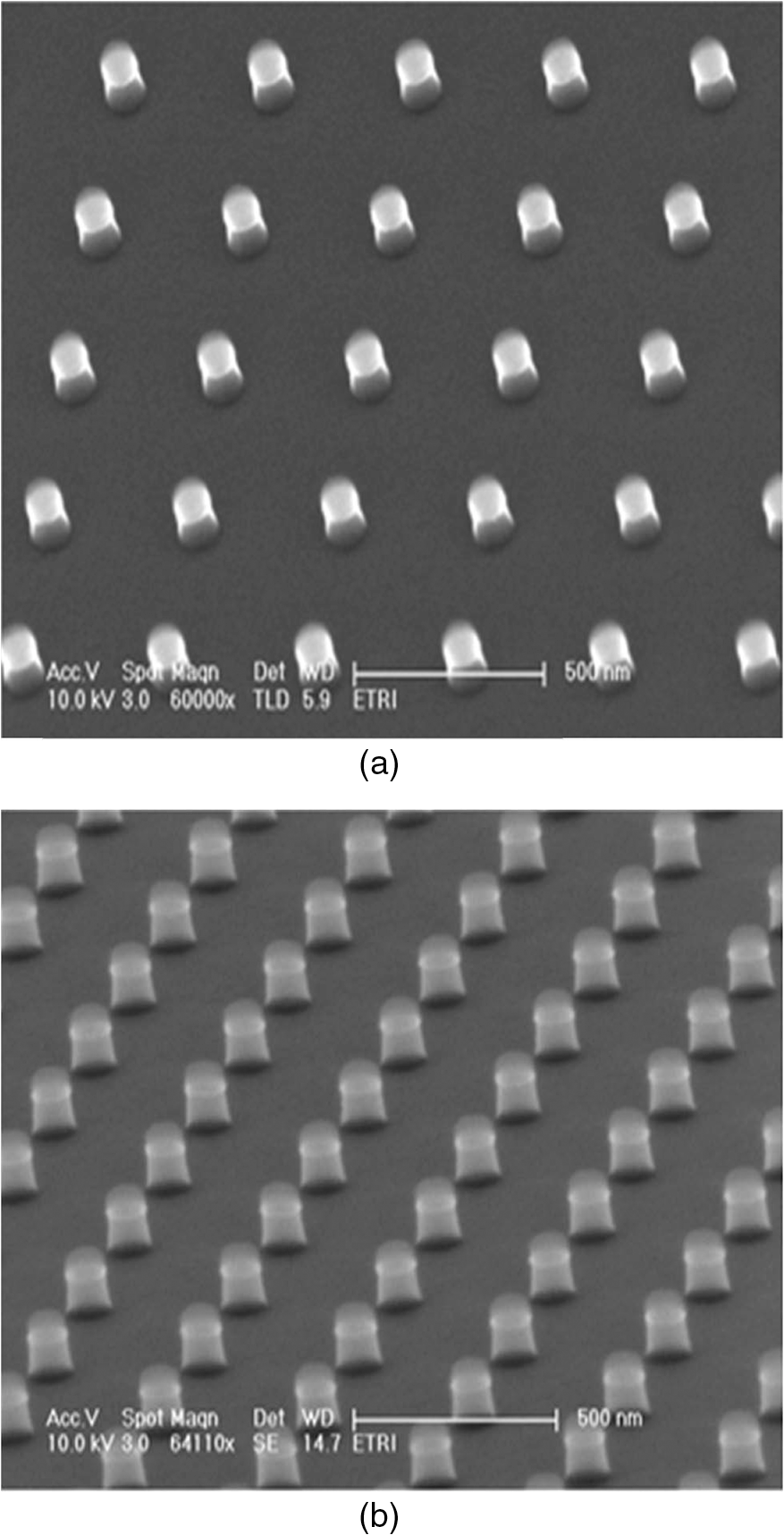 During the contact printing on the polymer film having a thickness of 100 nm with the silicon master molds, we could control the processing parameter values like temperature, pressure, and staying times for the precise and reliable nanoimprinting patterns. We found that there was the thermal reflow of about 20% from the initial contacted surface naturally. Figure 4 shows the SEM photograph of the precise patterning and the reflow of the polymer after the nanoimprinting processes using the nano molds with a diameter of 100 nm and with a height of 100 nm. We could obtain about 30 nm patterns using the thermal reflow phenomenon of the polymer resist, even with the pole structures of a diameter of 50 nm. Using the nanopatterned polymer resist with a thickness of 50 nm as an etch mask, we could pattern the about 30-nm diametered nanopores in array on the 50-nm thick silicon nitride ultrathin membrane as shown in Fig. 5(a). Fig. 4SEM photograph of polymer structure profile (a) for the silicon master with pole structures both of a height of 100 nm and of a diameter of 100 nm for the contact nanoimprinting and (b) a broken parts of the structures showing the thermal reflow of the polymer with the slide fillet parts after nanoimprinting.  Fig. 5Pictures with illustrations along with the SEM images employing the reflown polymer as an etch mask and an anisotropic etching protocol in order to form nanopores precisely and uniformly: (a) after nanopatterning on polymer, (b) after reactive ion etch using combination, the distribution of minimal nanohole diameters on (c) the upper side and (d) the bottom side of the membrane. Hole size data were extracted from 320 and 360 holes which were selected randomly from numerous holes shown in the upper SEM and the bottom SEM images, respectively, from (b).  As for RIE processes, in which the external energy in the form of radio frequency power drives the chemical reaction, fluorine compounds (like , , , and ) are usually utilized for the SiN etch reactant gases.27 The fluorine free radicals from the dissociation of fluorine compounds are mainly responsible for the desired silicon nitride etching. However, the fluorine plasma SiN etching reactions goes on spontaneously (i.e., diffusion-driven), not needing ionic bombardment. Thus, the fluorine free radicals give high etch rates, but by themselves generate etch profiles that are nearly isotropic (the lateral etch rate is nearly equal to the vertical etch rate). Therefore, it is not proper for controlling precisely nanopores’ diameter and distributing uniformly, especially in several tens of nanoscale thicknesses. Especially, the bombardment of mixed Ar free radicals at the etched surface can makethe consumption of reactants which have to diffuse into the regions being etched easy and facilitate diffusion of the reaction products away from the etched feature, and result in anisotropic and perpendicular etch profile.27 By simply adjusting the composition of the reactant mixture, anisotropy can be achieved to get the etch profile with the vertical feature. In this experiment, we have selected an gas flow ratio of at 55°C to achieve a designed and vertical feature.23 The etch rate of gas mixture to SiN was about and to the polymer about . The experimental etch results are shown in Fig. 5 through SEM pictures and etch profiles employing the anisotropic etching protocols after nanopatterning on the polymer (a), anisotropic etch using combination (b), and the distribution of minimal nanohole diameters on (c) the upper side and (d) the bottom side of the membrane. Hole size data were extracted from 320 and 360 holes, which were selected randomly from numerous holes shown in the upper SEM and the bottom SEM images, respectively, from Fig. 5(b). As a result, it shows that polymer nanopatterns with about 30-nm diameter have been transferred to the etch profile of the nanopores directly while maintaining the patterned diameter of about 30 nm. An average minimal diameter of the nanohole array is 29.8 nm and the standard deviation is 4.3 nm. The etch holes’ distribution is controlled uniformly for the use of the membrane nanopores. The difference between the diameters of the bottom (29.8 nm) and upper (46.8 nm) hole windows is known to be caused by the variations in the consumption of etch reactants (which must diffuse into the regions being etched), changes in the amount of ion bombardment at the etched surfaces, and potentially diffusion of the reaction products away from the etched features.28 Thus, the nanohole diameter in the upper part is wider than that in the bottom. These phenomena could also be taken into account to design the reduction of the pore sizes in this experiment. Further decrease in diameter would be possible with the further deposition of SiN thin film on the fabricated membrane nanosieves.9 Also, there are increasing needs to integrate sensors or imaging devices on the devices, in this case, the micro- and nano-fabrication protocols consisting of high temperature processes and harsh chemicals are indispensable. We thus checked the proper chemical and thermal stabilities, and it can endure harsh conditions like high temperature up to 800°C for 1 h. Furthermore, it was endurable to many aggressive and strong chemicals like high-concentrated piranha (), potassium hydroxide (KOH), HF, HCl, and nitric acid () after dipping nanopores for 30 min at room temperature (the data are not shown in this article).29 Finally, we believe that the micro- and nano-fabrication method can be applicable to the pressure-driven nanobio sensing or imaging devices at the microscale and nanoscale and lab-on-a-chip technology. 4.ConclusionWe have presented a size-reduction fabrication method of SiN membrane nanopores () for mass production combining a nanoimprinting protocol mainly and an anisotropic RIE with the perpendicular feature and precise size controlling ability. With holes’ diameter of about 30 nm and thickness of about 50 nm, opening factors of about 6% are achieved. Nanoimprinting process as well as asymmetric RIE etch protocols for precise and uniform nanosieves on SiN membrane are implemented by combining the natural thermal reflow of about 20% from the initial contacted polymer surface and the bombardment of mixed Ar free radicals with the chemical etch of fluorine free radical gases. As a result, it shows that the polymer nanopatterns with about 30-nm diameter have been transferred to the etch profile of the nanoholes directly while maintaining the uniformity as well as the patterned diameter size. The average minimal diameter of the nanohole array is 29.8 nm and the standard deviation is 4.3 nm. The difference between the diameters of bottom (29.8 nm) and upper (46.8 nm) hole windows is caused by the variations in the consumption of etch reactants, changes in the amount of ion bombardment at the etched surfaces, and potentially diffusion of the reaction products away from the etched features. The contact imprinting master can be used continually for the generation of nanopores patterns simply and easily. The fabrication method of ultrathin membrane nanosieves can make it possible to facilitate the usage in pressure-driven nanobio sensing and imaging devices at the microscale and lab-on-a-chip technologies. AcknowledgmentsThis work was supported by the R&D program (K13282, Development of Diagnostic Equipment for Blood Stasis), and the Converging Research Center Program (2013K000367) through Ministry of Science, ICT and Future Planning (MSIP), Republic of Korea. ReferencesB. M. Venkatesanet al.,
“Nanopore sensors for nucleic acid analysis,”
Nat. Nanotechnol., 6
(10), 615
–624
(2011). http://dx.doi.org/10.1038/nnano.2011.129 1748-3387 Google Scholar
S. Howorka,
“Sequence-specific detection of individual DNA strands using engineered nanopores,”
Nat. Biotechnol., 19
(7), 636
–639
(2001). http://dx.doi.org/10.1038/90236 NABIF9 1087-0156 Google Scholar
S. Ding,
“Capturing single molecules of immunoglobulin and ricin with an aptamer-encoded glass nanopore,”
Anal. Chem., 81
(16), 6649
–6655
(2009). http://dx.doi.org/10.1021/ac9006705 ANCHAM 0003-2700 Google Scholar
G. V. Soniet al.,
“Detection of nucleosomal substructures using solid-state nanopores,”
Nano Lett., 12
(6), 3180
–3186
(2012). http://dx.doi.org/10.1021/nl301163m NALEFD 1530-6984 Google Scholar
M. P. Jonssonet al.,
“Plasmonic nanopore for electrical profiling of optical intensity landscapes,”
Nano Lett., 13
(3), 1029
–1033
(2013). http://dx.doi.org/10.1021/nl304213s NALEFD 1530-6984 Google Scholar
J. Hanet al.,
“Molecular sieving using nanofilters: past, present, and future,”
Lab Chip, 8
(1), 23
–33
(2008). http://dx.doi.org/10.1039/b714128a LCAHAM 1473-0197 Google Scholar
T. R. Gaborskiet al.,
“High-performance separation of nanoparticles with ultrathin porous nanocrystalline silicon membranes,”
ACS Nano, 4
(11), 6973
–6981
(2010). http://dx.doi.org/10.1021/nn102064c 1936-0851 Google Scholar
C. C. Striemeret al.,
“Charge- and size-based separation of macromolecules using ultrathin silicon membranes,”
Nature, 445
(7129), 749
–753
(2007). http://dx.doi.org/10.1038/nature05532 NATUAS 0028-0836 Google Scholar
H. D. Tonget al.,
“Silicon nitride nanosieve membrane,”
Nano Lett., 4
(2), 283
–287
(2004). http://dx.doi.org/10.1021/nl0350175 NALEFD 1530-6984 Google Scholar
D. S. Leeet al.,
“Construction of membrane sieves using stoichiometric and stress-reduced multilayer films,”
ETRI J., 34
(2), 226
–234
(2012). http://dx.doi.org/10.4218/etrij.12.1711.0013 1225-6463 Google Scholar
D. H. Choiet al.,
“Use of a columnar metal thin film as a nanosieve with sub-10 nm pores,”
Adv. Mater., 24
(32), 4408
–4413
(2012). http://dx.doi.org/10.1002/adma.201200755 ADVMEW 0935-9648 Google Scholar
B. M. Venkatesanet al.,
“DNA sensing using nanocrystalline surface-enhanced nanopore sensors,”
Adv. Funct. Mater., 20
(8), 1266
–1275
(2010). http://dx.doi.org/10.1002/adfm.v20:8 AFMDC6 1616-3028 Google Scholar
T. R. Gaborskiet al.,
“High-performance separation of nanoparticles with ultrathin porous nanocrystalline silicon membranes,”
ACS Nano, 4
(11), 6973
–6981
(2010). http://dx.doi.org/10.1021/nn102064c 1936-0851 Google Scholar
C. A. Merchantet al.,
“DNA translocation through graphene nanopores,”
Nano Lett., 10
(8), 2915
–2921
(2010). http://dx.doi.org/10.1021/nl101046t NALEFD 1530-6984 Google Scholar
G. F. Schneideret al.,
“DNA translocation through graphene nanopores,”
Nano Lett., 10
(8), 3163
–3167
(2010). http://dx.doi.org/10.1021/nl102069z NALEFD 1530-6984 Google Scholar
M. Houtet al.,
“Controlling nanopore size, shape, and stability,”
Nanotechnology, 21
(11), 115304
(2010). http://dx.doi.org/10.1088/0957-4484/21/11/115304 NNOTER 0957-4484 Google Scholar
C. J. Loet al.,
“Fabrication of symmetric sub-5 nm nanopores using focused ion and electron beams,”
Nanotechnology, 17
(13), 3264
–3267
(2006). http://dx.doi.org/10.1088/0957-4484/17/13/031 NNOTER 0957-4484 Google Scholar
C. C. Harrellet al.,
“Conical nanopore membranes: controlling the nanopore shape,”
Small, 2
(2), 194
–198
(2006). http://dx.doi.org/10.1002/(ISSN)1613-6829 1613-6829 Google Scholar
H. Leeet al.,
“Full wafer scale near zero residual nano-imprinting lithography using UV curable monomer solution,”
Microelectron. Eng., 77
(1), 42
–47
(2005). http://dx.doi.org/10.1016/j.mee.2004.08.008 MIENEF 0167-9317 Google Scholar
A. Schleunitzet al.,
“Full fabrication of 3D nanoimprint stamps with continuous reliefs using dose-modulated electron beam lithography and thermal reflow,”
J. Micromech. Microeng., 20
(9), 09502
(2010). http://dx.doi.org/10.1088/0960-1317/20/9/095002 JMMIEZ 0960-1317 Google Scholar
H. Schiftet al.,
“Shape control of polymer reflow structures fabricated by nanoimprint lithography,”
Microelectron. Eng., 88
(1), 87
–92
(2011). http://dx.doi.org/10.1016/j.mee.2010.08.029 MIENEF 0167-9317 Google Scholar
T. Leveder,
“Reflow of supported sub-100 nm polymer films as a characterization process for Nanoimprint lithography,”
Microelectron. Eng., 88
(8), 1867
–1870
(2011). http://dx.doi.org/10.1016/j.mee.2011.01.078 MIENEF 0167-9317 Google Scholar
D. S. Leeet al.,
“Microfabrication of SiN membrane nanosieve using anisotropic reactive ion etching (ARIE) with an gas flow,”
J. Nanosci. Nanotechnol., 11
(5), 4511
–4516
(2011). http://dx.doi.org/10.1166/jnn.2011.3631 JNNOAR 1533-4880 Google Scholar
X. Yanget al.,
“Micromachined membrane particle filters,”
Sens. Actuators, A, 73
(1–2), 184
–191
(1999). http://dx.doi.org/10.1016/S0924-4247(98)00269-6 SAAPEB 0924-4247 Google Scholar
S. Kuiperet al.,
“Development and applications of very high flux microfiltration membranes,”
J. Membr. Sci., 150
(1), 1
–8
(1998). http://dx.doi.org/10.1016/S0376-7388(98)00197-5 JMESDO 0376-7388 Google Scholar
C. J. M. van Rijnet al.,
“Deflection and maximum load of microfiltration membrane sieves made with silicon micromachining,”
J. Microelectromech. Syst., 6
(1), 48
–54
(1997). http://dx.doi.org/10.1109/84.557530 JMIYET 1057-7157 Google Scholar
G. T. A. Kovacs, Micromachined Transducers, 79 McGraw-Hill, New York
(1998). Google Scholar
G. T. A. Kovacs, Micromachined Transducers, 67 McGraw-Hill, New York
(1998). Google Scholar
G. T. A. Kovacs, Micromachined Transducers, 90 McGraw-Hill, New York
(1998). Google Scholar
BiographyDae-Sik Lee is a principal researcher in the BioMED Team at ETRI, Daejeon, Republic of Korea. He received his PhD in electronic engineering from Kyungpook National University, Korea, in 2000 and a PhD in nanoscience and nanoengineering in the Department of Electronic and Photonic Systems, Waseda University, Japan, 2009. His research interests include the design, fabrication, and characterization of BioMEMS and biomedical devices, microfluidic devices, lab-on-a-chip, their systems, and nanoengineering. Hyun-Woo Song received his PhD degree in semiconductor optics from Korea Advanced Institute of Science and Technology (KAIST) in 1999. He joined ETRI, Korea, and is currently a principal researcher of Medical Device Research Section. His research experiences are in the area of biomedical optics, biomedical optical system, and semiconductor optical devices. His current research foci are the medical tomographic imaging module and its semiconductor optical sources for optical coherence tomography and photoacoustic tomography. Choon-Gi Choi received his PhD degree from Université d’Orléans, France, in 1996. He is currently a director at Creative Research Center for Graphene Electronics in Electronics and Telecommunications Research Institute (ETRI) and an adjunct professor at the Department of Advanced Device Technology in University of Science and Technology (UST), Korea. He is also an associate editor of the journal Nanoconvergence, published by Springer. His research interests are graphene electronics and optoelectronics, metamaterials, nanophotonics, nanoimprint lithography. |


