|
|
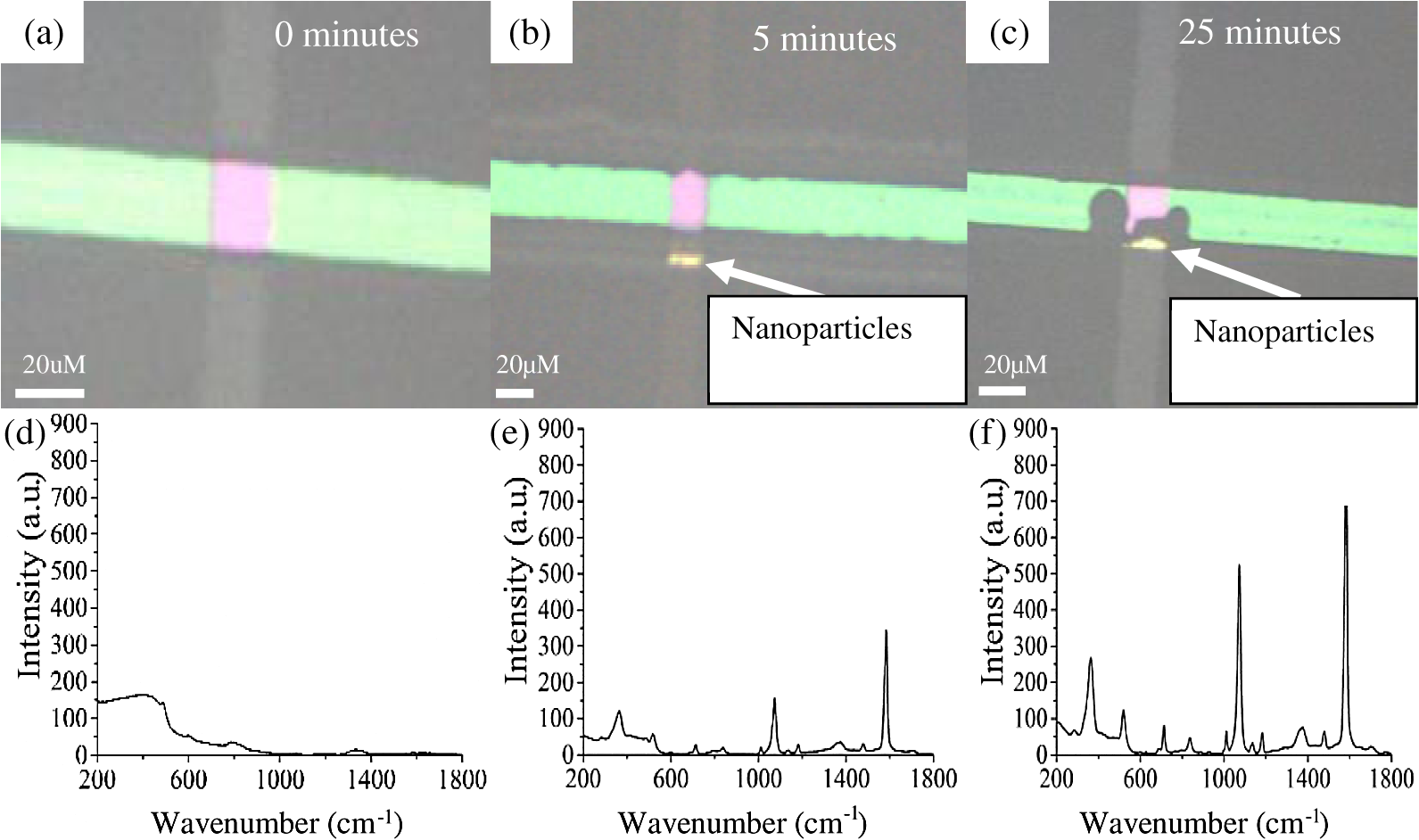
1.IntroductionSurface-enhanced Raman spectroscopy (SERS) is an optical technique that can be used to detect analytes at low concentrations.1 Raman spectroscopy provides rotational and vibrational energy information about the molecule adsorbed to the surface, and, because of the significant enhancement factor from the metal surface, SERS can be used for trace analysis.2–7 The enhancements seen from SERS allow examination of molecules in the nano-molar concentration range and below in solution, giving SERS the potential to become a good analytical method for biosensing. The nanoparticles used for SERS can be optimized to help produce a stronger enhancement. Their composition, size, capping agent, and morphology can all be altered to engineer a desired SERS signal.8–11 For example, nanocubes, nanospheres, nanobars, and nanostars are a few of the nanoparticle morphologies that have been engineered specifically to produce SERS enhancements, each having a unique effect on the Raman scattered light.12–17 Silver and gold colloids have also been analyzed using different sizes, preparation methods, and concentrations of analyte or reporter molecules attached to the nanoparticle.18–22 To increase the Raman scattering event probability further, various mechanical methods have been used to make the nanoparticles aggregate together, which causes strong enhancements to occur.23 One mechanical aggregation method was that of Hwang et al., in which an optoelectrofluidic device was used to create plasmonic aggregates aligned at the laser beam spot and produce strong enhancements. However, their device is a complex system that requires an alternating current voltage device to drive it.24 Chrimes et al.25 used a dielectrophoresis approach to trap nanoparticles by changing the frequency and voltage to force nanoparticles to aggregate at certain locations. While this method does produce many enhancements at the desired locations, this approach requires the user to tune the frequency and voltage depending on the size and composition of the nanoparticle.25 Zhou et al.26 have investigated microchannels with a valve system that, when closed, traps the nanoparticles. However, due to the large size of the microchannel with respect to the nanoparticle size, the position of the aggregates is not always in the same location. Therefore, the user has to move the objective around to find the aggregates manually.26 Wang et al.27 developed micro- to nanochannels to capture nanoparticle clusters forming only at the micro- to nanojunction. They were able to produce SERS enhancements at their micro- to nanochannel junction with detection limits down to 10 pM. In this paper, not only is the design and manufacture of the micro- to nanochannel described, its utility is also demonstrated by using it to analyze and compare colloidal spherical gold, gold-silver nanocages, silica-gold nanoshells, and silver nanocubes in order to determine which nanoparticle has better postfunctionalization utility for providing the best enhancement. 2.Materials and Methods2.1.Nanoparticle CharacterizationTransmission electron microscope (TEM; JEOL JEM-2010 TEM) images of the 60-nm gold spheres, 60-nm silver-gold nanocages, 100-nm silver nanocubes, and 135-nm silica-gold nanoshells (Nanocompsix) were collected before functionalization to show the nanoparticles’ size and morphology. A Tecan ultraviolet visible (UV/VIS) spectrometer was used to measure the extinction spectra of each nanoparticle solution. A NanoSight particle tracking system (NanoSight, LM10, nanoparticle size microscope) was used to characterize the particle concentrations and particle size distribution. SERS spectra were also recorded (Thermo Scientific, DXR Raman microscope) to show the enhancement capabilities of the different nanoparticles in the micro- to nanochannels. All other reagents mentioned hereafter were purchased from Sigma-Aldrich. 2.2.Nanoparticle SynthesisThe 60-nm nanocages were obtained from the Xia Group at Washington University and were prepared using the galvanic reduction and an AgNP template method as described by Chen et al. in Ref. 28. Chloroauric acid () is added to a solution of Ag nanoparticles, causing the galvanic reduction to occur, and the nanoparticle takes on the shape of the Ag template. The nanocage templates can be engineered to be various shapes, allowing the colloid’s local surface plasmon resonance wavelength to be tuned from 500 to 1200 nm based on the molar ratio of the to Ag. The 100-nm silver nanocubes were obtained from the Wu group at Texas A&M University and prepared from seeding growth synthesis. They were synthesized from silver nitrate with copper (ll) chloride as a seeding agent in a polyvinylpyrrolidone (PVP) pentanediol solution, as described in Ref. 29. Ethanol is used to quench the reaction and wash out any remaining reactants. The cubes in the ethanol solution are then diluted with a PVP/ultrapure solution and filtered. Lastly, the nanocubes are washed with ethanol and concentrated to the present concentration. The 60-nm gold nanospheres were purchased from Polysciences Inc., and the silica-gold nanoshells were purchased from Nanocomposix. 2.3.Raman Reporter Preparation and Functionalization to the NanoparticlesFive milligrams of MBA powder was mixed with 45 ml of 200 proof ethanol and sonicated for 30 min, yielding a MBA/ethanol solution. Another dilution was performed from the initial stock solution by adding deionized water, yielding a final MBA concentration of . Each of the four types of nanoparticles was mixed at a volumetric ratio with of MBA/ethanol solution and vortexed for . After 1 h, the nanoparticles were washed by adding 200-proof ethanol to the solution to fill up a 1.5-ml centrifuge tube and centrifuging for 30 min. Following the centrifugation, the supernatant was removed, and deionized water was added to fill the 1.5-ml centrifuge tube, which was then centrifuged for 30 min. The supernatant was removed again and the nanoparticles were resuspended in of deionized water to match the initial volume of the nanoparticle MBA solution to keep the concentration the same. The washing steps remove the previous capping agent on the nanoparticles, citrate, or PVP, depending on the nanoparticle, and replace them with MBA. 2.4.Micro- to Nanochannel SynthesisThe optofluidic micro- to nanochannel device was fabricated using photolithography and etching. The fabrication process is shown in Fig. 1. The substrate is a double-sided polished fused silica wafer with a thickness (Mark Optics Inc., Santa Ana, California). For the fabrication of the microchannel, 50 nm of silicon nitride () was deposited onto the fused silica wafer using plasma-enhanced chemical vapor deposition. The photoresist is then spin-coated on the to make the wide microchannel pattern. We used a plastic mask to make the channels, and the smallest width for plastic masks is . However, it is possible to use a metal mask, and the smallest width for these is typically . After UV exposure, the at the patterned area is etched completely off by dry etching, leaving only the photoresist on the wafer. Following this step, the photoresist wafer is submerged into the buffer of etchant, which etches away the exposed silica in the microchannel pattern down to . Once the inlet and outlet holes for the microchannel are drilled, the photoresist is stripped off by acetone and the layer is removed completely by hot phosphoric acid (, 160°C), which completes the microchannel fabrication. For the fabrication of the nanochannel, the photoresist is spin-coated directly onto a fused silica wafer, and a wide nanochannel is patterned onto the wafer. Afterward, carbon tetrafluoride () reactive ion etching is used to make a 40-nm deep nanochannel into the wafer. Following the removal of the photoresist from the nanochannel wafer using acetone, the wafer with the microchannel and the wafer with the nanochannel are thoroughly cleaned via piranha solution and annealed at 1050°C for 10 h. The annealing process permanently bonds the substrates by thermal fusion bonding. The completed optofluidic device shown in Fig. 2 uses a micro- to nanochannel junction structure to trap the nanoparticles. The microfluidic channel has a depth of and a width of . The nanofluidic channel has a depth of 40 nm and width of . The mechanism for introducing and aggregating the nanoparticles in the micro- to nanochannel is shown in Fig. 2(d). After pipetting the sample solution into the microchannel inlet, the solution is drawn into the optofluidic device by capillary force.30 All four nanoparticles have diameters that are larger than the 40 nm micro- to nanojunction; therefore, they form clusters at the micro- to nanojunction, which is the SERS detection area. Fig. 2Schematic diagram of the optofluidic device showing the (a) top view of the micro- to nanochannel junction, schematic, and bright field image; (b) three-dimensional side view of micro- to nanochannel; (c) side view of micro- to nanochannel; and (d) side view of micro- to nanochannel with nanoparticles aggregating.  2.5.Surface-Enhanced Raman Spectroscopy CollectionMicro- to nanochannel SERS spectra were collected using a Thermo Scientific DXR Raman confocal microscope. The samples were excited using a diode laser with a power of 24 mW through a Olympus microscope objective configured with an grating. Samples were exposed 30 times for 5 s for a total integration of 150 s. 3.Results and Discussion3.1.Nanoparticle ImagingNanoparticle composition, size, capping agent, and morphology are the major components that affect the SERS signal; therefore, we begin by looking at morphology using a TEM image for each nanoparticle. Figure 3 shows the shape and size of the four nanoparticles used in this study. Gold nanospheres were determined to be 60 nm and spherical in shape. Au–Ag nanocages were determined to be 60 nm but are cube-shaped and porous. The gold-silver nanoshells have a silica core with a gold shell, are 135 nm, and are spherical. The silver nanocubes are 100 nm and cubed in shape. A NanoSight system (Malvern Instruments, Worcestershire, UK) was used to show the concentration, average particle size, and particle distribution for all nanoparticles to verify the particle size and ensure the nanoparticles being compared had the same concentration of 147 pM. 3.2.Extinction Spectra for NanoparticlesThe extinction spectra of the four nanoparticles were analyzed in this study to assess their resonance around the 785-nm laser used in this study. Even if the nanoparticle extinction spectra are not perfectly in resonance with the 780-nm extinction laser, they will be shifted to the near-infrared region through mechanical aggregation. In the absence of mechanical aggregation, this shift has also been achieved by chemical aggregation using NaCl and can also be accomplished using elements that have a positive charge, which attract the negative surface charge of the citrate on the surface of the gold nanoparticles.31,32 However, the SERS experiments discussed in this paper do not need NaCl due to the forced aggregation by the micro- to nanochannel. In addition, as with some of the particles here, the colloidal nanoparticle systems can be engineered to have their extinction spectra tuned to a particular wavelength. For instance, the nanoshells have a dielectric core and are surrounded by a metal shell such as gold or silver, and their extinction spectra are tuned depending on the size and composition of the core/shell ratio.33 Nanocages can also have their size, and therefore their optical properties, tuned by controlling the molar ratio between the silver template and when making the nanocages.28 For the silver nanocubes, the extinction spectra are tuned primarily by the edge curvature of the nanocubes and particle size.34 Lastly, gold colloid extinction spectra that do not resonate with the excitation source were chosen to illustrate how the forced aggregation at the micro- to nanochannel shifts the extinction spectra to the desired wavelength to produce SERS signals. The extinction spectra of each type of colloid was collected before and after the addition of MBA, as shown in Fig. 4. As depicted in the data, MBA at this concentration does not cause a shift in the extinction spectra of the four nanoparticles, which is due to the electrostatic affect from MBA that prevents the nanoparticles from aggregating. Figure 4 also shows that the nanoshells, nanocages, and nanocubes are in resonance with the 780-nm excitation wavelength. The gold nanospheres are the only nanoparticle not engineered to be in resonance with the excitation wavelength, but a shift in the extinction spectra does occur when they aggregate. Also, when NaCl is used, aggregation and a shifted extinction spectra occur for the gold colloid, as shown in Fig. 4(b). NaCl was also added to the other three nanoparticles before the addition of MBA to assess its effect on these particles. In these instances, the salt did not shift the extinction spectra, due to the steric stabilization provided by the capping agent PVP on the surface of these nanoparticles, unlike the electrostatically stabilizing citrate capping agent on gold nanospheres. It is important to note that the maximum intensity for the extinction spectra does not need to be directly over the excitation wavelength. Le Ru et al.35 presented work that shows the extinction spectra is one indicator for the enhancement of the corresponding SERS signal when looking at a single nanoparticle. When using aggregation, the localized resonances at various locations on the nanoparticle are more effective for creating enhancements than the location of the extinction spectra maximum peak relative to the excitation wavelength because of the dimers, and so on, created.35 3.3.Micro- to Nanochannel Device DesignThe fluidic flow called capillary flow in this newly designed micro- to nanochannel is caused by capillary force. To describe the capillary flow in rectangular microchannels, we combine the Navier–Stoke’s equations with Young–Laplace equation. We consider only two-dimensional flow in the microchannel because the height of the microchannel is substantially smaller than the width. Therefore, we discuss capillary flow in the microchannel in the -direction and -direction. From the equations, we get the average velocity [Eq. (1)] and time [Eq. (2)] the fluid takes to get to the micro- to nanochannel junction. The detailed process is described in the Appendix. where is the average velocity, is the position in the -direction, is the time for the fluid to arrive at the micro- to nanojunction, is the height of the microchannel, is the viscosity of the fluid, is the width of the microchannel, is the surface tension, is the contact angle, and is the total length from inlet to micro- to nanojunction.Based on Eqs. (1) and (2), the calculated capillary flow velocity was determined to be , and the time for the fluid to arrive at the junction was 0.153 s. The physical properties of the fluid, such as viscosity, contact angle, and surface tension, all remain constant. To improve on Wang’s design,27 our microchannels were constructed with shallower channels that are in depth and in width. (Wang’s design was in depth and in width.) The velocity in our new micro- to nanochannel is two times faster than Wang’s design, and the travel time is also reduced. Our micro- to nanochannel is designed using an innovative one-step etching process rather than multiple etching steps. Previously, two etching processes, dry and wet etchings, were required for making nanochannels and microchannels on a single wafer. In this approach, the two channels are patterned on two different wafers and, as a result, a single etching process is used to make nano- and microchannels on each wafer. Hot wet etching is specifically used to remove the layer. One-step etching is advantageous over the previous method because multiple etching steps cause damage to the surface. Dry or wet etching would create an uneven surface because energetic plasma or active radicals damage the surface randomly. Photoresist protection is not effective to secure the surface from these active chemicals if multiple etching processes are required. Once the surface is damaged, it will affect the thermal fusion bonding process, which causes difficulties when trying to permanently bond two substrates. Therefore, multiple etching procedures should be avoided for bonding processes. One-step etching also produces a stronger bond between the two quartz wafers.36 Lastly, these channels are designed for one-time use only. 3.4.Micro- to Nanochannel Surface-Enhanced Raman Spectroscopy AnalysisAll four nanoparticles were analyzed in the micro- to nanochannel. A solution of of functionalized nanoparticles was pipetted into the microchannel inlet, and SERS scans were taken over time at the nanochannel junction. Each functionalized nanoparticle was evaluated in three different micro- to nanochannels. Figures 5(a)–5(c) show the micro- to nanochannel junction at 0 min, 5 min, and 25 min, respectively. The horizontal channel is the microchannel, and the vertical channel is the nanochannel. At time 0, no nanoparticles have been inserted into the micro inlet, only deionized water. Figure 5(b) shows the micro- to nanochannel junction 5 min after of the functionalized silver nanoparticles were pipetted into the micro inlet. The nanoparticles, silver nanocubes in this example, are clearly seen aggregating at the micro- to nanojunction. Figure 5(c) shows the micro- to nanochannel 25 min after the initial solution was inserted into the micro inlet, and the larger size of the aggregates formed at the junction can be visualized compared with the 5-min aggregate size. In Fig. 5(d), a Raman scan was taken to show the baseline signal of the micro- to nanochannel. Figure 5(e) shows the SERS spectra at 5 min, with the MBA peaks easily discernible relative to the background spectrum seen in Fig. 5(d). Figure 5(f) shows the increase in SERS signal that occurs after more nanoparticles have moved to the micro- to nanochannel junction. The increase is due to the forced aggregation at the micro- to nanochannel junction, which creates many “hot spots” that form between the nanoparticles, silver nanocubes in this case, that are all in close proximity to each other.8 Lastly, Figs. 6(a)–6(d) show the SERS spectrum of all four functionalized nanoparticles over time at the micro- to nanochannel junction. The main reason the silver nanocubes have the largest enhancement among the four nanoparticles is likely due to the morphology. The cube shape of the silver nanoparticles provides several corners to form hot spots, each giving a significantly increased SERS signal. To calculate the enhancement factor, the Raman spectra of 100-mM MBA dissolved in ethanol was used to compare with the intensity from of MBA adsorbed to the surfaces of the various nanoparticles. Specifically, enhancement factors for the nanoparticles were calculated using Eq. (3) to be , , , and for silver nanocubes, gold nanospheres, gold-silver nanocages, and silica-gold nanoshells, respectively37 where is the SERS intensity, is the intensity of MBA at 100-mM concentration, is the concentration of 100 mM MBA in moles, and is the concentration of MBA in moles.4.ConclusionThis data shows that, in the micro- to nanochannel, silver nanocubes have a larger enhancement factor than gold nanospheres, silica-gold nanoshells, or gold-silver nanocages. The larger size of the silver nanoparticles contributed to greater SERS intensities due to the larger nanoparticles having more localized surface plasmons propagating on their surfaces, which are in resonance with the excitation wavelength. The cubed shape of the silver nanocubes also allows more hot spots to form than the spherical nanoshells and gold nanospheres.8,9 The nanocubes have several corners to form hot spots when in the vicinity of another nanoparticle, providing more places where the hot spots can occur to yield strong SERS enhancements relative to the spherical nanoparticles. Although the nanocages have the same cubed shape, the nanocubes give stronger enhancements than the cube-shaped nanocages due to the plasmon dampening that occurs between the gold and silver used to engineer the nanocages.38 Altogether, the size, tuned extinction spectra, and many hot spots formed all contribute to the silver nanocubes having the strongest average SERS intensity compared with the other nanoparticles. Overall, four different nanoparticles were analyzed to determine which produces the strongest SERS signal in a micro- to nanochannel. It has been shown that of MBA functionalized 100-nm silver nanocubes exhibited the largest enhancement when using the micro- to nanochannel. Using the SERS method with nanoparticles functionalized with RRMs and microfluidic channels for aggregation has applications for detection of a number of different biomarkers. Specifically, just a few of the blood biomarker experiments that are underway in our group include: the detection of cardiac troponin for determining if a patient has had a heart attack; the detection of bisphenol A to assess toxicity, and the detection of citrulline as a measure of gut function and metabolism. AppendicesAppendixTo describe the capillary flow in rectangular microchannels, we combine the Navier–Stoke’s equations [Eqs. (4) and (5)] with the Young–Laplace equation [Eq. (9)] using substitution. From these equations, we get the average velocity [Eq. (12)] and time [Eq. (13)] the fluid takes to get to the micro- to nanochannel junction. The above process is described in Fig. 7. Navier–Stokes -direction -direction where is the fluid velocity in the -direction, is the fluid velocity in the -direction, is the pressure, is the density of fluid, is the viscosity of fluid, is the gravity, and is the time.Assumption for simplified Navier–Stokes’ Equation: (1) incompressible fluid, (2) steady state, (3) Laminar flow, and (4) Newtonian fluid.
Therefore, Navier–Stokes’ equation is simplified to Eq. (7). The boundary condition in the -direction is when , which gives . The solution to Eq. (7) is displayed in Eq. (8) According to the Young–Laplace equation, the capillary pressure () in a rectangular microchannel can be described as Here, is the surface tension, is the curvature of width, is the curvature of height, is the width of the microchannel, is the height of the microchannel, and is the contact angle.Substituting Young’s equation [Eq. (9)] into the solution of the simplified Navier–Stokes’ equation [Eq. (8)], the capillary flow rate in the rectangular microchannel can be described as The average velocity of capillary flow in the microchannel can be defined by the volume flow rate in the microchannel Capillary flow can be defined by the physical meaning of velocity, speed, or the average velocity where is the average velocity, : is the position in -direction, is the time for the fluid to arrive at the micro- to nanojunction, is the height of the microchannel, is the viscosity of the fluid, is the width of the microchannel, is the surface tension, is the contact angle, and is the total length from the inlet to the micro- to nanojunction.Using the equations above with the constants below, we find the average velocity and time for the sample to get to the micro- to nanochannel junction. We also show the average velocity and time for Wang’s paper further below for comparative purposes: The dimensions of the micro- to nanochannel mentioned in Wang’s paper: AcknowledgmentsResearch reported in this publication was supported by the National Institute of Environmental Health Sciences of the National Institutes of Health under Grant No. P30ES023512. The content is solely the responsibility of the authors and does not necessarily represent the official views of the National Institutes of Health. ReferencesK. C. Bantz et al.,
“Recent progress in SERS biosensing,”
Phys. Chem. Chem. Phys., 13
(24), 11551
–11567
(2011). http://dx.doi.org/10.1039/c0cp01841d Google Scholar
J. N. Anker et al.,
“Biosensing with plasmonic nanosensors,”
Nat. Mater., 7
(6), 442
–453
(2008). http://dx.doi.org/10.1038/nmat2162 Google Scholar
D. Cialla et al.,
“Surface-enhanced Raman spectroscopy (SERS): progress and trends,”
Anal. Bioanal. Chem., 403
(1), 27
–54
(2012). http://dx.doi.org/10.1007/s00216-011-5631-x Google Scholar
K. Hering et al.,
“SERS: a versatile tool in chemical and biochemical diagnostics,”
Anal. Bioanal. Chem., 390
(1), 113
–124
(2008). http://dx.doi.org/10.1007/s00216-007-1667-3 Google Scholar
B. Sharma et al.,
“SERS: materials, applications, and the future,”
Mater. Today, 15
(1–2), 16
–25
(2012). http://dx.doi.org/10.1016/S1369-7021(12)70017-2 MATOBY 1369-7021 Google Scholar
W. E. Smith,
“Practical understanding and use of surface enhanced Raman scattering/surface enhanced resonance Raman scattering in chemical and biological analysis,”
Chem. Soc. Rev., 37
(5), 955
–964
(2008). http://dx.doi.org/10.1039/b708841h Google Scholar
S. Xu et al.,
“Surface-enhanced Raman scattering studies on immunoassay,”
J. Biomed. Opt., 10
(3), 031112
(2005). http://dx.doi.org/10.1117/1.1915487 Google Scholar
S. Abalde-Cela et al.,
“Surface-enhanced Raman scattering biomedical applications of plasmonic colloidal particles,”
J. R. Soc. Interface, 7
(Suppl. 4), S435
–S450
(2010). http://dx.doi.org/10.1098/rsif.2010.0125.focus Google Scholar
N. D. Israelsen, C. Hanson and E. Vargis,
“Nanoparticle properties and synthesis effects on surface-enhanced Raman scattering enhancement factor: an introduction,”
Sci. World J., 2015 1
–12
(2015). http://dx.doi.org/10.1155/2015/124582 Google Scholar
C. M. Cobley et al.,
“Gold nanostructures: a class of multifunctional materials for biomedical applications,”
Chem. Soc. Rev., 40
(1), 44
–56
(2011). http://dx.doi.org/10.1039/B821763G Google Scholar
M. Kahraman et al.,
“Experimental parameters influencing surface-enhanced Raman scattering of bacteria,”
J. Biomed. Opt., 12
(5), 054015
(2007). http://dx.doi.org/10.1117/1.2798640 Google Scholar
J. M. McLellan et al.,
“The SERS activity of a supported Ag nanocube strongly depends on its orientation relative to laser polarization,”
Nano Lett., 7
(4), 1013
–1017
(2007). http://dx.doi.org/10.1021/nl070157q NALEFD 1530-6984 Google Scholar
C. E. Talley et al.,
“Surface-enhanced Raman scattering from individual Au nanoparticles and nanoparticle dimer substrates,”
Nano Lett., 5
(8), 1569
–1574
(2005). http://dx.doi.org/10.1021/nl050928v NALEFD 1530-6984 Google Scholar
Q. Zhang et al.,
“Synthesis of Ag nanobars in the presence of single-crystal seeds and a bromide compound, and their surface-enhanced Raman scattering (SERS) properties,”
Langmuir, 28
(24), 9047
–9054
(2012). http://dx.doi.org/10.1021/la300253a LANGD5 0743-7463 Google Scholar
C. G. Khoury and T. Vo-Dinh,
“Gold nanostars for surface-enhanced Raman scattering: synthesis, characterization and optimization,”
J. Phys. Chem. C, 112
(48), 18849
–18859
(2008). http://dx.doi.org/10.1021/jp8054747 Google Scholar
C. M. Cobley et al.,
“Shape-controlled synthesis of silver nanoparticles for plasmonic and sensing applications,”
Plasmonics, 4
(2), 171
–179
(2009). http://dx.doi.org/10.1007/s11468-009-9088-0 1557-1955 Google Scholar
C. L. Nehl, H. Liao and J. H. Hafner,
“Optical properties of star shaped gold nanoparticles,”
Nano Lett., 6
(4), 683
–688
(2006). http://dx.doi.org/10.1021/nl052409y NALEFD 1530-6984 Google Scholar
A. Kandakkathara, I. Utkin and R. Fedosejevs,
“Surface-enhanced Raman scattering (SERS) detection of low concentrations of tryptophan amino acid in silver colloid,”
Appl. Spectrosc., 65
(5), 507
–513
(2011). http://dx.doi.org/10.1366/10-06150 Google Scholar
I. A. Larmour, K. Faulds and D. Graham,
“SERS activity and stability of the most frequently used silver colloids,”
J. Raman Spectrosc., 43
(2), 202
–206
(2012). http://dx.doi.org/10.1002/jrs.v43.2 JRSPAF 0377-0486 Google Scholar
T. Makiabadi et al.,
“Preparation, optimization, and characterization of SERS sensor substrates based on two-dimensional structures of gold colloid,”
Plasmonics, 5
(1), 21
–29
(2010). http://dx.doi.org/10.1007/s11468-009-9110-6 1557-1955 Google Scholar
R. Stiufiuc et al.,
“SERS-active silver colloids prepared by reduction of silver nitrate with short-chain polyethylene glycol,”
Nanoscale Res. Lett., 8
(1), 47
(2013). http://dx.doi.org/10.1186/1556-276X-8-47 NRLAAD 1556-276X Google Scholar
E. Tourwé, K. Baert and A. Hubin,
“Surface-enhanced Raman scattering (SERS) of phthalic acid and 4-methyl phthalic acid on silver colloids as a function of pH,”
Vib. Spectrosc., 40
(1), 25
–32
(2006). http://dx.doi.org/10.1016/j.vibspec.2005.06.005 VISPEK 0924-2031 Google Scholar
M. Li et al.,
“Plasmonic nanorice antenna on triangle nanoarray for surface-enhanced Raman scattering detection of hepatitis B virus DNA,”
Anal. Chem., 85
(4), 2072
–2078
(2013). http://dx.doi.org/10.1021/ac303387a Google Scholar
H. Hwang et al.,
“In situ dynamic measurements of the enhanced SERS signal using an optoelectrofluidic SERS platform,”
Lab Chip, 11
(15), 2518
–2525
(2011). http://dx.doi.org/10.1039/c1lc20277d LCAHAM 1473-0197 Google Scholar
A. F. Chrimes et al.,
“Dielectrophoresis-Raman spectroscopy system for analysing suspended nanoparticles,”
Lab Chip, 11
(5), 921
–928
(2011). http://dx.doi.org/10.1039/c0lc00481b LCAHAM 1473-0197 Google Scholar
J. Zhou et al.,
“Convenient formation of nanoparticle aggregates on microfluidic chips for highly sensitive SERS detection of biomolecules,”
Anal. Bioanal. Chem., 402
(4), 1601
–1609
(2012). http://dx.doi.org/10.1007/s00216-011-5585-z Google Scholar
M. Wang et al.,
“Optofluidic device for ultra-sensitive detection of proteins using surface-enhanced Raman spectroscopy,”
Microfluid. Nanofluid., 6
(3), 411
–417
(2009). http://dx.doi.org/10.1007/s10404-008-0397-y Google Scholar
J. Chen et al.,
“Gold nanocages: engineering their structure for biomedical applications,”
Adv. Mater., 17
(18), 2255
–2261
(2005). http://dx.doi.org/10.1002/(ISSN)1521-4095 ADVMEW 0935-9648 Google Scholar
H. J. Wu et al.,
“Membrane-protein binding measured with solution-phase plasmonic nanocube sensors,”
Nat. Methods, 9
(12), 1189
–1191
(2012). http://dx.doi.org/10.1038/nmeth.2211 Google Scholar
M. N. Hamblin et al.,
“Selective trapping and concentration of nanoparticles and viruses in dual-height nanofluidic channels,”
Lab Chip, 10
(2), 173
–178
(2010). http://dx.doi.org/10.1039/B916746C LCAHAM 1473-0197 Google Scholar
S. Abdali et al.,
“Resonance surface enhanced Raman optical activity of myoglobin as a result of optimized resonance surface enhanced Raman scattering conditions,”
J. Phys. Condens. Matter, 19
(28), 285205
(2007). http://dx.doi.org/10.1088/0953-8984/19/28/285205 JCOMEL 0953-8984 Google Scholar
F. Liu et al.,
“Surface-enhanced Raman scattering study of riboflavin on borohydride-reduced silver colloids: dependence of concentration, halide anions and pH values,”
Spectrochim. Acta. Part A, 85
(1), 111
–119
(2012). http://dx.doi.org/10.1016/j.saa.2011.09.043 Google Scholar
N. Halas,
“Playing with plasmons: tuning optical resonant properties of metallic nanoshells,”
MRS Bull., 30
(5), 362
–367
(2005). http://dx.doi.org/10.1557/mrs2005.99 MRSBEA 0883-7694 Google Scholar
N. C. Worstell et al.,
“Binding cooperativity matters: a GM1-Like ganglioside-cholera toxin B subunit binding study using a nanocube-based lipid bilayer array,”
PLoS One, 11
(4), e0153265
(2016). http://dx.doi.org/10.1371/journal.pone.0153265 POLNCL 1932-6203 Google Scholar
E. C. Le Ru, C. Galloway and P. G. Etchegoin,
“On the connection between optical absorption/extinction and SERS enhancements,”
Phys. Chem. Chem. Phys., 8
(26), 3083
–3087
(2006). http://dx.doi.org/10.1039/b605292d Google Scholar
D. Radziuk and H. Moehwald,
“Highly effective hot spots for SERS signatures of live fibroblasts,”
Nanoscale, 6
(11), 6115
–6126
(2014). http://dx.doi.org/10.1039/c4nr00594e NANOHL 2040-3364 Google Scholar
L. Tian, N. Gandra and S. Singamaneni,
“Monitoring controlled release of payload from gold nanocages using surface enhanced Raman scattering,”
ACS Nano, 7
(5), 4252
–4260
(2013). http://dx.doi.org/10.1021/nn400728t ANCAC3 1936-0851 Google Scholar
BiographyBrian M. Walton is a PhD candidate in the Department of Biomedical Engineering at Texas A&M University. His research focus is on developing point-of-care optical biosensors using surface-enhanced Raman spectroscopy. He has presented his research to SPIE twice and has been recognized by BMES with an Innovation and Career Development Award. He is also an Alfred P. Sloan Foundation Fellow. He earned a Bachelor of Science in physics from Florida A&M University. Po-Jung Huang is pursuing his PhD in the Department of Material Science and Engineering at Texas A&M University. His research focus is on the development of microfluidic devices for single molecular detection, especially protein complexes and biotoxins. He also concentrates on manufacturing cell and bacteria microenvironment via hydrogel for cancer research and waste water treatment. He is a current member of SPIE. Jun Kameoka is an associate professor in the Department of Electrical and Computer Engineering, Material Science and Engineering at Texas A&M University. He is also affiliated as an adjunct professor with the Frontier Medical Engineering Department at Chiba University and Tokyo Jikei School of Medicine in Japan. His expertise is nano- and microfluidics, micro- and nanosensors, and actuators. He has been awarded 10 U.S. and Japanese patents and published over 100 journal articles and conference proceedings. Gerard L. Cote is the director for the Center for Remote Health Technologies and Systems and holds the Charles H. and Bettye Barclay professorship within the Department of Biomedical Engineering at Texas A&M University. He is recognized as a worldwide expert in optical sensing for diagnostic and biomedical monitoring applications. He is a fellow of four societies; coauthor of over 300 publications, proceedings, patents, and abstracts; and cofounder of four medical device companies. |