

|
|
|
Optical coherence tomography (OCT) is considered an essential noninvasive optical imaging technique for providing microstructural and functional information with respect to biological tissues in real time.1 Advancements in broadband light sources, sensitive detectors, and real-time computing techniques enabled OCT to achieve excellent performance with high spatial resolution and real-time volumetric display.2–4 Thus, it is a premier medical instrument for diagnosing ophthalmic diseases.5,6 In addition, clinical researchers in various medical fields, including dermatology, cardiology, oncology, and gastroenterology, utilize the OCT technique in alternative promising medical diagnostic devices.7–9 Furthermore, OCT is also utilized in nonmedical applications, such as nondestructive inspection tools in industrial fields for thin film-based products and agriculture.10–13 The acquisition of cross-sectional and volumetric OCT data involves scanning of sample OCT beams at the desired target region. However, the use of motorized stages in the first OCT scanner is limited because of its large size and low scanning speed, which cause motion artifacts.3,14 These issues necessitated advanced scanners for clinical implementation. Recently, galvanometer scanners were utilized in real-time commercial OCT systems because of their linear scanning patterns, fast scanning abilities, and precise positioning.15,16 However, the use of the galvanometer scanners to develop endoscopic or small-sized handheld probes for imaging internal organs (e.g., esophagus and bronchus) is difficult owing to their oriented configurations containing two-axial ( and axes) servo motors and relatively large size of the galvanometer scanners. To compensate these bottlenecks, various types of microelectromechanical system (MEMS) scanners (e.g., electrostatic,17 electromagnetic,17 piezoelectric,18 and electrothermal types19) were introduced for endoscopic and handheld probes.20 Although their advantages include small form factors and high speed scanning abilities, the complex fabrication process, relatively high costs, and suitable operating conditions requirements present drawbacks for true clinical implementation and commercialization. Particularly, normal silicon-based MEMS scanners required various manufacturing procedures, including photolithography, thin-film deposition, masking, etching, and metallization. Hence, these multifarious fabrication steps resulted in complexities in the MEMS scanner structures and high manufacturing costs. Moreover, it was difficult to use the MEMS scanners in humid environments. In this study, a two-axis polydimethylsiloxane (PDMS)-based electromagnetic MEMS (2A-PDMS-MEMS) scanning mirror using a simple and cost-effective soft lithography microfabrication process was developed. The performance of the 2A-PDMS-MEMS scanning mirror, such as the scanning pattern and the AC/DC response, was measured. Finally, the 2A-PDMS-MEMS scanning mirror was applied in a spectral-domain optical coherence tomography (SD-OCT) system as an optical scanning mirror. In vivo microstructural information of an individual’s fingertips and palm was successfully visualized. The schematic of the 2A-PDMS-MEMS scanning mirror is shown in Fig. 1(a). Table 1 indicates the design parameters of the 2A-PDMS-MEMS scanning mirror. A major consideration of the design involves fabrication simplicity and a large scanning angle, in most conditions. The PDMS was utilized as the base material of the structure in consideration of these matters. The scanning mirror could be driven under a wide range of AC/DC conditions given the considerable elasticity of the rubber-like PDMS material. In addition, soft lithography that utilizes the PDMS stamping is an easy and cost-effective process in replicating the microstructure. Figure 1(b) shows the PDMS structural layer for the scanning mirror. The detailed fabrication steps of the MEMS scanning mirror are described by previous studies.21,22 The fabrication steps involved cutting a master mold for the PDMS body and acrylic supporting structures by using a micromilling machine. Then, the PDMS (Sylgard 184, Dow Corning, United States) was poured on the master mold and was cured in a convection oven at 80°C. The PDMS body defined the shape of the scanner and offered two pairs of torsional hinges along the and axes. An additional acrylic supporter formed a rigid gimbal structure, which separated two scanning motions along the and axes. This was followed by plasma treatment that enhanced the surface bonding between the acrylic supporter and the PDMS body. The aluminum mirror developed by e-beam evaporation on a thin silicon wafer had a large reflecting area (i.e., along the and axes), and it was positioned at the center of the PDMS body. Four neodymium magnets were fixed inside the PDMS body and strong laboratory-made electromagnets were aligned with each magnet. Finally, the PDMS structural layer and the block of electromagnets were assembled with an adhesive. Electromagnetic attractive and repulsive forces between the neodymium magnets in the movable PDMS body and electromagnets in an aluminum block [Fig. 1(c)] were utilized to create torsional scanning motions of the mirror. The size of the fabricated 2A-PDMS-MEMS scanning mirror was along the , , and axes, respectively. Figure 1(d) shows the photograph of the 2A-PDMS-MEMS scanning mirror. Fig. 1Design and fabricaton of 2A-PDMS-MEMS scanning mirror. (a) 3-D schematic design of 2A-PDMS-MEMS scanning mirror; (b) disassembled PDMS structral layer; (c) aligned electromagnets and permanent magnets; and (d) photograph of fabricated 2A-PDMS-MEMS scanning mirror. AM, aluminum mirror; PM, permanent magnet; EM, electromagnet.  Table 1Design parameters of the 2A-PDMS-MEMS scanning mirror.
Figure 2(a) shows an experimental setup to demonstrate the scanning characteristics of the fabricated 2A-PDMS-MEMS scanning mirror, including the maximum scanning angle and resonance frequency under the DC/AC conditions. The driving voltages for the electromagnets along the and axes were controlled by the analog outputs of a data acquisition system (NI PCIe-6321, National Instruments, United States). A current amplifier circuit with a high-current op-amp (OPA2544, Texas Instruments, United States) was used to provide sufficient current to the coils. At various amplitudes and frequencies of the driving voltage, the maximum scanning angle was determined using Eq. (1) as follows: where is the vertical distance between the mirror and the sample and is the measured scanning length. First, the scanning angle was obtained by increasing the driving voltage from 0 V to 10 V at the DC condition [Fig. 2(b)]. As shown in the linear fitting from the experimental data, the applied voltage and the scanning angle displayed a linear relationship. Note that the resistance change of each electromagnet is negligible (i.e., with a DC voltage of 10 V). The maximum scanning angles along the and axes were at 4 V and at 10 V, respectively. To avoid sticking of the permanent magnet to the electromagnet, the maximum applied voltages are limited to 4 and 10 V along the and axes, respectively. A thick torsional hinge along the axis resulted in higher stiffness, which in turn resulted in a smaller scanning angle than that along the axis. The scanning angles along the and axes were measured by increasing the driving frequency to show the frequency response at a fixed voltage of [Fig. 2(c)]. The resonance frequencies of the MEMS scanning mirror were 82 and 57 Hz along the and axes, respectively. Compared to shear modulus of silicon (e.g., ) in conventional MEMS technology, the low shear modulus of PDMS (e.g., ) mainly resulted in low resonance frequencies, which were exactly in the operational range of the fabricated scanning mirror (i.e., 50 to 100 Hz). Both raster and Lissajous scanning patterns were successfully demonstrated [Figs. 2(d) and 2(e)] because of the AC/DC scanning characteristics. The raster scanning pattern is obtained at the following driving conditions: 2 V at 4 Hz along the -axis and 3 V at 96 Hz along the axis, respectively. The Lissajous scanning pattern is obtained at the following driving conditions: 3 V at 81 Hz () along the -axis and 3 V at 74 Hz () along the -axis, respectively. In the raster scanning mode for a dense pixel number, the linear and high scanning angles of the mirror are preferred at the DC condition. Although B-scan and volumetric images could be easily acquired using the raster scan, fast and wide imaging is possible using the Lissajous scan. In this study, the raster scan was used only to obtain accurate B-scan and volumetric OCT images. The 2A-PDMS-MEMS scanning mirror has the advantages of a larger field of view (FOV) at smaller driving voltages compared with the commercial MEMS mirror used in other OCT systems.23 For instance, the maximum FOV of the system is along the and axes with an optical focal length of 50 mm and a driving voltage of 4 and 10 V along and axes, respectively. By contrast, a commercial product with a 2.4-mm mirror size has the FOV of with a driving voltage range of 0 to 100 V.23 The measured current flow in coils is about 21 mA at 2 V and 53 mA at 5 V during in vivo imaging. Although this current flow is high and causes damages in tissues with direct contact,24 the coils in the MEMS scanner are fully electrically insulated. In addition, the current flows in the previously reported OCT MEMS scanners range from 20 to 100 mA.25 Thus, we believe that the electrical power of our system is low enough for biomedical applications.Fig. 2Scanning characteristics of 2A-PDMS-MEMS scanning mirror. (a) Experimental setup; (b) maximum scanning angle versus input voltage; (c) frequency response at AC voltage; (d) raster scan pattern; and (e) lissajous scan pattern. AMP, amplifier; DAQ, data acquisition board.  The conventional SD-OCT system was implemented to prove the feasibility of the 2A-PDMS-MEMS scanning mirror in the OCT. However, the existing galvanometer scanning mirror was replaced with the 2A-PDMS-MEMS scanning mirror. Figure 3(a) shows a schematic of the SD-OCT system based on the 2A-PDMS-MEMS scanning mirror. A broadband light beam (SLD-351-HP3, Superlum, Ireland) with a center wavelength of 860 nm, bandwidth of 59.6 nm, and output power of 16.5 mW was delivered to the sample and the reference arms through a optical coupler (F850-40-50-APC, Thorlabs). The sample and reference arms were composed of identical collimators (F260APC-B, Thorlabs) and objective lenses (AC254-050-B, Thorlabs) to compensate for the dispersion. The 2A-PDMS-MEMS scanning mirror was applied to the sample arm for volumetric optical scanning. The interference signals were generated at different depths following the incident light reflected from both arms. The signals were captured by a laboratory-made line-camera-based spectrometer. The spectrometer consisted of a 2-in. achromatic lens (AC508-075-B, Thorlabs), a grating (HD , Wasatch Photonics), and a line-scan camera (SpL4096-140Km, Basler, Germany). The recorded OCT signals were converted to digital data through a frame grabber (PCIe-1429, National Instruments). The converted data were transformed into B-scan OCT images after additional signal processing involving k-linearization26 and fast Fourier transform was performed via LabView software. The spatial resolution was measured using a carbon fiber to evaluate the performance of the SD-OCT system. The measured lateral and axial resolutions were 23 and , which are close to the theoretical lateral (i.e., ) and axial (i.e., ) resolutions [Figs. 3(b) and 3(c)]. The sensitivity measured from a mirror sample is 108 dB. Finally, B-scan and volumetric OCT images of the human finger area were obtained. All human experimental procedures were conducted in accordance with protocols approved by the institutional review board of POSTECH. To acquire OCT images of a human finger, we recruited healthy volunteers. A sine waveform with a frequency of 11.8 Hz and an input voltage of 2 V were applied to obtain the B-scan OCT images along the axis. A sawtooth waveform with a frequency of 0.06 Hz and an input voltage of 5 V were utilized along the axis to operate a volumetric imaging mode. The acquired pixel size is along and axes, respectively. The imaging time was 17 s, and the FOV of the acquired image was along the and axes. The volumetric image data were reconstructed through a commercial 3-D rendering software (Amira 6, FEI). Fig. 3SD-OCT system setup and measured spatial resolution. (a) Schematic of the SD-OCT system at 860 nm with PDMS-based MEMS scanning mirror. (b) and (c) Measured lateral and axial resolution, respectively. SLD, superluminescent diode; DAQ, data acquisition board.  Figures 4(a) and 4(b) indicate the OCT images of the fingertips and palm, respectively. Figures 4(i), 4(ii), 4(iii), and Ref. 15 illustrate B-scan OCT images along the and axes, B-scan OCT images along the and axes, en-face OCT images along the and axes, and volumetric rendering OCT images, respectively. The B-scan OCT images clearly visualized the structural information of the skin surface, the epidermis, and the dermis. In addition, the fingertip patterns and sweat ducts were observed in Fig. 4(b). Fig. 4In vivo B-scan and volumetric OCT images of (a) human fingertips and (b) palm. (i) B-scan OCT images at the axes, (ii) B-scan OCT images at the axes, (iii) en-face OCT image at the axes, and (iv) volumetric OCT images. S, skin surface; EP, epidermis; D, dermis; SD, sweat duct. 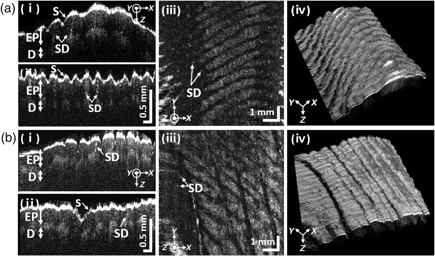 The two-axis electromagnetic MEMS scanning mirror using a flexible PDMS material was successfully demonstrated. This novel MEMS scanner provided a relatively cost effective and simple fabrication process for repetitive production when compared with the conventional MEMS process. Then, the characteristics of the 2A-PDMS MEMS scanning mirror, including the scanning pattern and the AC/DC response, were measured. Finally, the 2A-PDMS MEMS scanning mirror integrated with the SD-OCT system was evaluated by scanning a human subject’s fingertips and palm. The 2A-PDMS-MEMS scanning mirror is expected to play a crucial role in diverse optical imaging systems for fast translation and commercialization. Future research that could result in further improvements include the following: (1) compensation of a nonlinear and asymmetric scanning pattern of a scanning mirror, (2) utilization of multimodal optical imaging systems to provide comprehensive biological information, (3) further reduction in the size of the 2A-PDMS-MEMS scanning mirror for adapting an endoscopic regime, and (4) fabrication of a MEMS scanner with high resonance frequency to avoid environmental noises and achieve high speed imaging. Particularly, it is expected that a nonlinear scanning pattern, hysteresis, and cross-talks between two axes can be compensated by well-known feedback loop based control methods.27 AcknowledgmentsThis research was supported by the Ministry of Science, ICT and Future Planning (MSIP), Korea, under the “ICT Consilience Creative Program” (Grant No. IITP-R0346-16-1007) supervised by the Institute for Information & communications Technology Promotion (IITP), an NRF Engineering Research Center grant (NRF-2011-0030075), and an Industrial Technology Innovation Program (Grant No. 10048358) of the Ministry of Trade, Industry & Energy, Republic of Korea. This work was also supported by the National Research Foundation of Korea (NRF) grant funded by the Korean government (MSIP) (Grant No. 2015R1A2A1A14027903). ReferencesD. Huang et al.,
“Optical coherence tomography,”
Science, 254
(5035), 1178
–1181
(1991). http://dx.doi.org/10.1126/science.1957169 SCIEAS 0036-8075 Google Scholar
H. Jeong et al.,
“Ultra-fast displaying spectral domain optical Doppler tomography system using a graphics processing unit,”
Sensors, 12
(6), 6920
–6929
(2012). http://dx.doi.org/10.3390/s120606920 SNSRES 0746-9462 Google Scholar
C. Lee et al.,
“Combined photoacoustic and optical coherence tomography using a single near-infrared supercontinuum laser source,”
Appl. Opt., 52
(9), 1824
–1828
(2013). http://dx.doi.org/10.1364/AO.52.001824 APOPAI 0003-6935 Google Scholar
A. M. Zysk et al.,
“Optical coherence tomography: a review of clinical development from bench to bedside,”
J. Biomed. Opt., 12
(5), 051403
(2007). http://dx.doi.org/10.1117/1.2793736 JBOPFO 1083-3668 Google Scholar
C. Lee et al.,
“Stimulated penetrating keratoplasty using real-time virtual intraoperative surgical optical coherence tomography,”
J. Biomed. Opt., 19
(3), 030502
(2014). http://dx.doi.org/10.1117/1.JBO.19.3.030502 JBOPFO 1083-3668 Google Scholar
R. F. Spaide and C. A. Curcio,
“Anatomical correlates to the bands seen in the outer retina by optical coherence tomography: literature review and model,”
Retina, 31
(8), 1609
–1619
(2011). http://dx.doi.org/10.1097/IAE.0b013e3182247535 RETIDX 0275-004X Google Scholar
P. A. Testoni and B. Mangiavillano,
“Optical coherence tomography in detection of dysplasia and cancer of the gastrointestinal tract and bilio-pancreatic ductal system,”
World J. Gastroenterol., 14
(42), 6444
–6452
(2008). http://dx.doi.org/10.3748/wjg.14.6444 Google Scholar
X. Cai et al.,
“Investigation of neovascularization in three-dimensional porous scaffolds in vivo by a combination of multiscale photoacoustic microscopy and optical coherence tomography,”
Tissue Eng. Part C, 19
(3), 196
–204
(2012). http://dx.doi.org/10.1089/ten.tec.2012.0326 Google Scholar
E. Sattler, R. Kästle and J. Welzel,
“Optical coherence tomography in dermatology,”
J. Biomed. Opt., 18
(6), 061224
(2013). http://dx.doi.org/10.1117/1.JBO.18.6.061224 JBOPFO 1083-3668 Google Scholar
K. Wiesauer et al.,
“En-face scanning optical coherence tomography with ultra-high resolution for material investigation,”
Opt. Express, 13
(3), 1015
–1024
(2005). http://dx.doi.org/10.1364/OPEX.13.001015 OPEXFF 1094-4087 Google Scholar
C. Lee et al.,
“Optical sensing method for screening disease in melon seeds by using optical coherence tomography,”
Sensors, 11
(10), 9467
–9477
(2011). http://dx.doi.org/10.3390/s111009467 SNSRES 0746-9462 Google Scholar
C.-H. Lee et al.,
“The application of optical coherence tomography in the diagnosis of Marssonina blotch in apple leaves,”
J. Opt. Soc. Korea, 16
(2), 133
–140
(2012). http://dx.doi.org/10.3807/JOSK.2012.16.2.133 1226-4776 Google Scholar
S.-Y. Lee et al.,
“Application of optical coherence tomography to detect Cucumber green mottle mosaic virus (CGMMV) infected cucumber seed,”
Hortic. Environ. Biotechnol., 53
(5), 428
–433
(2012). http://dx.doi.org/10.1007/s13580-012-0071-x Google Scholar
J. M. Schmitt,
“Optical coherence tomography (OCT): a review,”
IEEE J. Sel. Top. Quantum Electron., 5
(4), 1205
–1215
(1999). http://dx.doi.org/10.1109/2944.796348 IJSQEN 1077-260X Google Scholar
M. Wojtkowski et al.,
“Three-dimensional retinal imaging with high-speed ultrahigh-resolution optical coherence tomography,”
Ophthalmology, 112
(10), 1734
–1746
(2005). http://dx.doi.org/10.1016/j.ophtha.2005.05.023 OPANEW 0743-751X Google Scholar
T. Wang et al.,
“Intravascular optical coherence tomography imaging at 3200 frames per second,”
Opt. Lett., 38
(10), 1715
–1717
(2013). http://dx.doi.org/10.1364/OL.38.001715 OPLEDP 0146-9592 Google Scholar
W. Jung et al.,
“Three-dimensional endoscopic optical coherence tomography by use of a two-axis microelectromechanical scanning mirror,”
Appl. Phys. Lett., 88
(16), 163901
(2006). http://dx.doi.org/10.1063/1.2195092 APPLAB 0003-6951 Google Scholar
K. H. Gilchrist et al.,
“Piezoelectric scanning mirrors for endoscopic optical coherence tomography,”
J. Micromech. Microeng., 19
(9), 095012
(2009). http://dx.doi.org/10.1088/0960-1317/19/9/095012 JMMIEZ 0960-1317 Google Scholar
A. Jain et al.,
“A two-axis electrothermal micromirror for endoscopic optical coherence tomography,”
IEEE J. Sel. Top. Quantum Electron., 10
(3), 636
–642
(2004). http://dx.doi.org/10.1109/JSTQE.2004.829194 IJSQEN 1077-260X Google Scholar
T.-H. Tsai et al.,
“Ultrahigh speed endoscopic optical coherence tomography using micromotor imaging catheter and VCSEL technology,”
Biomed. Opt. Express, 4
(7), 1119
–1132
(2013). http://dx.doi.org/10.1364/BOE.4.001119 BOEICL 2156-7085 Google Scholar
J. Y. Kim et al.,
“Fast optical-resolution photoacoustic microscopy using a 2-axis water-proofing MEMS scanner,”
Sci. Rep., 5 7932
(2015). http://dx.doi.org/10.1038/srep07932 SRCEC3 2045-2322 Google Scholar
J. Y. Kim et al.,
“A PDMS-based 2-axis waterproof scanner for photoacoustic microscopy,”
Sensors, 15
(5), 9815
–9826
(2015). http://dx.doi.org/10.3390/s150509815 SNSRES 0746-9462 Google Scholar
C. D. Lu et al.,
“Handheld ultrahigh speed swept source optical coherence tomography instrument using a MEMS scanning mirror,”
Biomed. Opt. Express, 5
(1), 293
–311
(2014). http://dx.doi.org/10.1364/BOE.5.000293 BOEICL 2156-7085 Google Scholar
R. M. Fish and L. A. Geddes,
“Conduction of electrical current to and through the human body: a review,”
ePlasty, 9 e44
(2009). Google Scholar
J. Sun and H. Xie,
“MEMS-based endoscopic optical coherence tomography,”
Int. J. Opt., 2011 1
–12
(2011). http://dx.doi.org/10.1155/2011/825629 Google Scholar
M. Jeon et al.,
“Full-range k-domain linearization in spectral-domain optical coherence tomography,”
Appl. Opt., 50
(8), 1158
–1163
(2011). http://dx.doi.org/10.1364/AO.50.001158 APOPAI 0003-6935 Google Scholar
H. W. Yoo, S. Ito and G. Schitter,
“High speed laser scanning microscopy by iterative learning control of a galvanometer scanner,”
Control Eng. Pract., 50 12
–21
(2016). http://dx.doi.org/10.1016/j.conengprac.2016.02.007 COEPEL 0967-0661 Google Scholar
BiographySehui Kim is a researcher in the Department of Creative IT Engineering, Pohang University of Science and Technology (POSTECH). She received her MS degree in the Department of Electrical Engineering from Kyugpook National University in 2014. She is interested in biomedical imaging including photoacoustic imaging and optical coherence tomography. Changho Lee has been a postdoctoral fellow at Johns Hopkins University (JHU) in Baltimore, USA, since 2016. Before joining JHU, he studied at the Kyungpook National University for his PhD degree. Recently, he investigated at the Pohang University of Science and Technology (POSTECH) as the postdoctoral fellow and research assistant professor. He focused on developing novel biomedical imaging modalities, such as optical coherence tomography, photoacoustic imaging, integrated optical imaging, and intraoperative surgical imaging. Jin Young Kim received his PhD in the Department of Mechanical Engineering at Pohang University of Science and Technology (POSTECH). He is working at POSTECH as a postdoctoral research associate. His research interests are development of novel photoacoustic imaging, multimodal optical imaging systems using MEMS devices, and their clinical applications. Jeehyun Kim is an associate professor of the School of Electrical Engineering at Kyungpook National University in Daegu, Republic of Korea. Before joining the school, he received his PhD degree in biomedical engineering from the University of Texas at Austin and researched at the University of California, Irvine, Beckman Laser Institute as a postdoctoral associate. His interests include the development of novel optical imaging technique, such as optical coherence tomography, and ultrahigh-speed optical imaging. Geunbae Lim received his BSc and MSc degrees in electronic engineering from Yeungnam University, Republic of Korea, in 1990 and 1992, respectively. He received his PhD in precision engineering from Tohoku University, Japan, in 1996. He joined the Microsystems Laboratory, Samsung Advanced Institute of Technology (SAIT), Korea. He is on the faculty of Pohang University of Science and Technology. His research interests are in the areas of nano/bio-MEMS. Chulhong Kim is currently an associate professor of Creative IT Engineering at Pohang University of Science and Technology, in the Republic of Korea. Before he joined the department, he was an assistant professor of biomedical engineering at the University at Buffalo, the State University of New York, from 2010 to 2013. He studied for his PhD and postdoctoral training at Washington University in St. Louis, Missouri. |
||||||||||||||||||||||||||||||||||||||||


